设计一个12V转3.3V,输出电流30mA的电源电路,由于项目对转化效率要求较高,所以不能采用低压差线性稳压LDO的方案。经过对比,TOREX的XC9264效率在此转化条件下效率可做到85%以上,比MPS等厂家同类型芯片效率做得高很多。

特性:
输入电压范围:3-18V(极限值20V)
FBVoltage: 0.75V
开关频率:500kHz,1.2MHz,2.2MHz
输出最大电流:0.5A
控制模式:PWM/PFM
软启动时间:由RC调节
保护:过流保护、内部锁定机制、热关机
输出、输入采用低ESR陶瓷电容
封装:SOT-25,USP-6C
典型电路图:
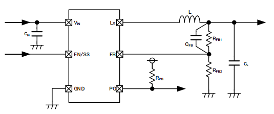
输出电压设定:Vout=Vfb*(Rfb1+Rfb2)/Rfb2 (注意Rfb1+Rfb2<1Mohm)
相位补偿加速电容(phase compensation speed-up capacitor):Cfb=1/(2∏*fzfb*Rfb1)

软启动时间设定:通过增加一个电容和一个电阻给EN/SS脚


内部结构框图:

内部功能模块:软启动电路、误差放大器、PWM比较器、斜坡电路、振荡器、相位补偿电路、限流电路、PFM脉冲调制电路、高低侧驱动、低电压锁定电路(UVLO)、门钳位电路、热关机电路(TSD)、内部供电电路
工作模式:输出电压反馈至FB引脚,与误差放大器比较后,误差放大器输出脉冲补偿,该信号输入PWM比较器,输出信号至驱动缓冲电路,从LX输出开关周期信号,从而稳定住电压。
Reference voltage source:该参考电流源提供参考电压确保输出电压稳定;
Oscillator circuit:斜坡电路决定了开关频率,有500KHZ,1.2MHZ或者2.2MHZ;
为避免自已翻译容易造成误解,以下摘抄datasheet英文原文:
Current limiting:The current limiting circuit of the XC9263/64 series monitors the current that flows through the High-side driver transistor and Low-side driver transistor, and when over-current is detected, the current limiting function activates.
① Low-side driver Tr. current limiting
The current in the Low-side driver Tr. is detected to equivalently monitor the bottom value of the coil current. The Low-side driver Tr. current limiting function prohibits the High-side driver Tr. from turning on in an over-current state where the bottom value of the coil current is higher than the Low-side driver Tr. current limit value ILIML. Control to lower the switching frequency fOSC is also performed. When the over-current state is released, normal operation resumes.
② High-side driver Tr. current limiting
The current in the High-side driver Tr. is detected to equivalently monitor the peak value of the coil current. The High-side driver Tr. current limiting function forcibly turns off the High-side driver Tr. when the peak value of the coil current reaches the High-side driver current limit value ILIMH. ILIML < ILIMH is set inside the IC, and therefore the Low-side driver Tr. current limiting function of ① above also detects the over-current state at this time. When the over-current state is released, normal operation resumes.
③ Over-current latch (Type A)
Type A turns off the High-side and Low-side driver Tr. when state ① or ② continues for 1.0ms (TYP.). The LX pin is latch-stopped at the GND level (0V).
The latch-stopped state only stops the pulse output from the Lx pin; the internal circuitry of the IC continues to operate. To restart after latch-stopping, L level and then H level must be input into the EN/SS pin, or VIN pin re-input must be performed (after lowering the voltage below the UVLO detection voltage) to resume operation by soft start.
The over-current latch function may occasionally be released from the current limit detection state by the effects of ambient noise, and it may also happen that the latch time becomes longer or latching does not take place due to board conditions. For this reason, place the input capacitor as close as possible to the IC.
Type B is an automatic recovery type that performs the operation of ① or ② until the over-current state is released.
Low side driver Tr. current limit value ILIML=0.7A (TYP.)
High-side driver Tr. current limit value ILIMH=1.1A (TYP.)

Soft-start function:
The reference voltage applied to the error amplifier is restricted by the start-up voltage of the EN/SS pin. This ensures that the error amplifier operates with its two inputs in balance, thereby preventing ON-time signal from becoming longer than necessary. Therefore, start-up time of the EN/SS pin becomes the set-time of soft-start. The soft-start time can be adjusted by adding a capacitor and a resistor to the EN/SS pin.
If the EN/SS pin voltage rises steeply without connecting CSS and RSS (RSS=0Ω), Output rises with taking the soft-start time of tss1=1.0ms (TYP.) which is fixed internally.
The soft-start function operates when the voltage at the EN/SS pin is between 0.3V to 2.5V. If the voltage at the EN/SS pin does not start from 0V but from a middle level voltage when the power is switched on, the soft-start function will become ineffective and the possibilities of large inrush currents and ripple voltages occurring will be increased.
Thermal shutdown:
The thermal shutdown (TSD) as an over current limit is built in the XC9263/64 series.When the junction temperature reaches the detection temperature, the driver transistor is forcibly turned off. When the junction temperature falls to the release temperature while in the output stop state, restart takes place by soft-start.
UVLO:
When the VIN pin voltage falls below 2.7V (TYP.), the driver transistor is forcibly turned off to prevent false pulse output due to instableoperation of the internal circuits. When the VIN pin voltage rises above 2.8V (TYP.), the UVLO function is released, the soft-start function activates, and output start operation begins. Stopping by UVLO is not shutdown; only pulse output is stopped and the internal circuits continueto operate.
Power good:
On USP-6C Package, the output state can be monitored using the power good function.When the FB voltage drops below 90% (TYP.), the PG pin outputs an "L" signal.The PG pin is an Nch open drain output, therefore a pull-up resistance (approx. 100kΩ) must be connected to the PG pin.