http://en.wikipedia.org/wiki/Chipset
Chipset
A chipset is a set of electronic components in an integrated circuit that manages the data flow between the processor, memory and peripherals. It is usually found in the motherboard of a computer. Chipsets are usually designed to work with a specific family of microprocessors. Because it controls communications between the processor and external devices, the chipset plays a crucial role in determining system performance.
Computers[edit]
In computing, the term chipset is commonly used to refer to a set of specialized chips on a computer's motherboard or an expansion card. In personal computers, the first chipset for the IBM PC AT was the NEAT chipset by Chips and Technologies for the Intel 80286 CPU.


In home computers, game consoles and arcade game hardware of the 1980s and 1990s, the term chipset was used for the custom audio and graphics chips. Examples include the Commodore Amiga's Original Chip Set or SEGA's System 16chipset.
Based on Intel Pentium-class microprocessors, the term chipset often refers to a specific pair of chips on the motherboard: the northbridge and thesouthbridge. The northbridge links the CPU to very high-speed devices, especially RAM and graphics controllers, and the southbridge connects to lower-speed peripheral buses (such as PCI or ISA). In many modern chipsets, the southbridge contains some on-chip integrated peripherals, such asEthernet, USB, and audio devices.
The manufacturer of a chipset often is independent from the manufacturer of the motherboard. Current manufacturers of chipsets for x86 motherboards include AMD, Broadcom, Intel, NVIDIA, SiS and VIA Technologies. Applecomputers and Unix workstations have traditionally used custom-designed chipsets. Some server manufacturers also develop custom chipsets for their products.
In the 1980s, Chips and Technologies pioneered the manufacturing of chipsets for PC-compatible computers. Computer systems produced since then often share commonly used chipsets, even across widely disparate computing specialties. For example, the NCR 53C9x, a low-cost chipset implementing a SCSI interface to storage devices, could be found in Unix machines such as the MIPS Magnum, embedded devices, and personal computers.
Move toward processor integration in PCs[edit]
Traditionally in x86 computers, the processor's primary connection to the rest of the machine is through the motherboard chipset's northbridge. The northbridge is directly responsible for communications with high-speed devices (System memory, and primary expansion buses such as PCIe, AGP, PCI cards being common examples) and conversely any system communication back to the processor. This connection between the processor and northbridge is traditionally known as thefront side bus (FSB). Requests to resources not directly controlled by the northbridge are offloaded to the southbridge - with the northbridge being an intermediary between the processor and the southbridge. The southbridge traditionally handles "everything else," generally lower speed peripherals and board functions (the largest being hard disk and storage connectivity) such as USB, parallel and serial communications. The connection between the northbridge and southbridge does not have a common name, but is usually a high speed interconnect proprietary to the chipset vendor. Thus any interaction between a CPU and main memory, any expansion device such as a graphics card(s), whether AGP, PCI or integrated into the motherboard, was directly controlled by the northbridge IC on behalf of the processor. This made processor performance highly dependent on the system chipset - especially the northbridge's memory performance and ability to shuttle this information back to the processor.
However in 2003 AMD's introduction the Athlon 64-bit series of processors[1] changed this. The Athlon64 marked the introduction of an integrated memory controller being incorporated into the processor itself allowing the processor to directly access and handle memory, negating the need for a traditional northbridge to do so. Intel followed suit in 2008 with the release of its Core i series CPUs and the X58 platform." In newer processors integration has further increased, primarily inclusion of the system's primary PCIe controller and integrated graphics directly on the CPU itself. As fewer functions are left un-handled by the processor itself, chipset venders have condensed the remaining north and southbridge functions into a single chip. Intel's version of this is the "Platform Controller Hub" (PCH), effectively an enhanced southbridge for the remaining peripherals, as traditional northbridge duties such as memory controller, expansion bus (PCIe) interface, and even on-board video controller are integrated into the CPU itself.
http://en.wikipedia.org/wiki/Northbridge_(computing)
Northbridge (computing)
|
|
This article needs additional citations for verification. (January 2008) |

The northbridge or host bridge was one of the two chips in the core logic chipset on a PC motherboard, used to manage data communications between a CPU and a motherboard. It is supposed to be paired with a second support chip known as a southbridge.
The northbridge was historically one of the two chips in the core logic chipset on a PC motherboard, the other being the southbridge. Increasingly these functions became integrated into the CPU chip itself, beginning with memory and graphics controllers. For Intel Sandy Bridge and AMD Accelerated Processing Unit processors introduced in 2011, all of the functions of the northbridge reside on the CPU.[1] When a separate northbridge is employed in older Intel systems, it is named memory controller hub (MCH) or integrated memory controller hub (IMCH) if equipped with an integrated VGA.
Separating the different functions into the CPU, northbridge, and southbridge chips was due to the difficulty of integrating all components onto a single chip.[2] In some instances, the northbridge and southbridge functions have been combined onto one die when design complexity and fabrication processes permitted it; for example, theNvidia GeForce 320M in the 2010 Macbook Air is a northbridge/southbridge/GPU combo chip.[3]
As CPU speeds increased, a bottleneck eventually emerged between the processor and the motherboard, due to limitations caused by data transmission between the CPU and its support chipset. Accordingly, starting with the AMD Athlon64 series CPUs (based on the Opteron), a new architecture was used where some functions of the north- and southbridge chips were moved to the CPU. Intel followed suit with their Core i series CPUs.
Overview[edit]
The northbridge typically handles communications among the CPU, in some cases RAM, and PCI Express (or AGP) video cards, and the southbridge.[4][5] Some northbridges also contain integrated video controllers, also known as aGraphics and Memory Controller Hub (GMCH) in Intel systems. Because different processors and RAM require different signaling, a given northbridge will typically work with only one or two classes of CPUs and generally only one type of RAM.
There are a few chipsets that support two types of RAM (generally these are available when there is a shift to a new standard). For example, the northbridge from the Nvidia nForce2 chipset will only work with Socket Aprocessors combined with DDR SDRAM; the Intel i875 chipset will only work with systems using Pentium 4 processors or Celeron processors that have a clock speed greater than 1.3 GHz and utilize DDR SDRAM, and the Intel i915g chipset only works with the Intel Pentium 4 and the Celeron, but it can use DDR or DDR2 memory.
Etymology[edit]
The name is derived from drawing the architecture in the fashion of a map. The CPU would be at the top of the map comparable to due north on most general purpose geographical maps. The CPU would be connected to the chipset via a fast bridge (the northbridge) located north of other system devices as drawn. The northbridge would then be connected to the rest of the chipset via a slow bridge (the southbridge) located south of other system devices as drawn.

Overclocking[edit]
The northbridge plays an important part in how far a computer can be overclocked, as its frequency is commonly used as a baseline for the CPU to establish its own operating frequency. This chip typically gets hotter as processor speed becomes faster, requiring more cooling. There is a limit to CPU overclocking, as digital circuits are limited by physical factors such as propagation delay which increases with (among other factors) operating temperature; consequently most overclocking applications have software-imposed limits on the multiplier and external clock setting.
Evolution[edit]
The overall trend in processor design has been to integrate more functions onto fewer components, which decreases overall motherboard cost and improves performance. The memory controller, which handles communication between the CPU and RAM, was moved onto the processor die by AMD beginning with their AMD64 processors and by Intel with their Nehalem processors. One of the advantages of having the memory controller integrated on the CPU die is to reduce latency from the CPU-to-memory.
Another example of this kind of change is Nvidia's nForce3 for AMD64 systems. It combines all of the features of a normalsouthbridge with an Accelerated Graphics Port (AGP) port and connects directly to the CPU. On nForce4 boards it was marketed as a media communications processor (MCP).
AMD Accelerated Processing Unit processors feature full integration of northbridge functions onto the CPU chip, along with processor cores, memory controller and graphics processing unit (GPU). This was an evolution of the AMD64, since the memory controller was integrated on the CPU die in the AMD64.
The northbridge was replaced by the system agent introduced by the Sandy Bridge microarchitecture in 2011, which essentially handles all previous Northbridge functions.[6] Intel’s “Sandy Bridge” processors feature full integration of northbridge functions onto the CPU chip, along with processor cores, memory controller and graphics processing unit (GPU). This was a further evolution of the Westmere architecture, which also featured a CPU and GPU in the same package.[7]
http://en.wikipedia.org/wiki/Southbridge_(computing)
Southbridge (computing)

The southbridge is one of the two chips in the core logic chipset on a personal computer (PC) motherboard, the other being the northbridge. The southbridge typically implements the slower capabilities of the motherboard in a northbridge/southbridge chipset computer architecture. In Intel chipset systems, the southbridge is namedInput/Output Controller Hub (ICH). AMD, beginning with its Fusion APUs, has given the label FCH, or Fusion Controller Hub, to its southbridge.
The southbridge can usually be distinguished from the northbridge by not being directly connected to the CPU. Rather, the northbridge ties the southbridge to the CPU. Through the use of controller integrated channel circuitry, the northbridge can directly link signals from the I/O units to the CPU for data control and access.
Contents
[hide]Current status[edit]
Due to the push for System-on-a-chip (SoC) processors, modern devices increasingly have the northbridge integrated into the CPU die itself; examples are Intel's Sandy Bridge and AMD's Fusion processors (both released in 2011). The southbridge is redundant and was replaced by the Platform Controller Hub, all southbridge features were taken over by the PCH. Intel's Haswell launched in 2013 further stripped the southbridge off, remaining I/O functions are managed by the Lynx Point chipset.[1]
Overview[edit]
A southbridge chipset handles all of a computer's I/O functions, such as USB, audio, serial, the system BIOS, the ISA bus, the interrupt controller and the IDE channels.[2] Different combinations of Southbridge and Northbridge chips are possible,[3] but these two kinds of chips must be designed to work together;[4][5] there is no industry-wide standard for interoperability between different core logic chipset designs. Traditionally, the interface between a northbridge and southbridge was the PCI bus. The main bridging interfaces used now are DMI (Intel) andUMI (AMD).
Etymology[edit]
The name is derived from drawing the architecture in the fashion of a map and was first described as such with the introduction of the PCI Local Bus Architecture in 1991. At Intel, the authors of the PCI specification viewed the PCI local bus as being at the very centre of the PC platform architecture (i.e., at the Equator).
The northbridge extends to the north of the PCI bus backbone in support of CPU, Memory/Cache, and other performance-critical capabilities. Likewise the southbridge extends to the south of the PCI bus backbone and bridges to less performance-critical I/O capabilities such as the disk interface, audio, etc.
The CPU is located at the top of the map at due north. The CPU is connected to the chipset via a fast bridge (the northbridge) located north of other system devices as drawn. The northbridge is connected to the rest of the chipset via a slow bridge (the southbridge) located south of other system devices as drawn.
Although the current PC platform architecture has replaced the PCI bus backbone with faster I/O backbones, the bridge naming convention remains.
Functionality[edit]
The functionality found in a contemporary southbridge includes:[5]
- PCI bus. The PCI bus support includes the traditional PCI specification, but may also include support for PCI-X andPCI Express.
- ISA bus or LPC Bridge. Though the ISA support is rarely utilized, it has interestingly managed to remain an integrated part of the modern southbridge. The LPC Bridge provides a data and control path to the Super I/O (the normal attachment for the keyboard, mouse, parallel port, serial port, IR port, and floppy controller) and FWH (firmware hub which provides access to BIOS flash storage).
- SPI bus. The SPI bus is a simple serial bus mostly used for firmware (e.g., BIOS) flash storage access.
- SMBus. The SMBus is used to communicate with other devices on the motherboard (e.g., system temperature sensors, fan controllers).
- DMA controller. The DMA controller allows ISA or LPC devices direct access to main memory without needing help from the CPU.
- Interrupt controllers such as 8259A and/or I/O APIC. The interrupt controller provides a mechanism for attached devices to get attention from the CPU.
- Mass storage controllers such as PATA and/or SATA. This typically allows direct attachment of system hard drives.
- Real-time clock. The real time clock provides a persistent time account.
- Power management (APM and ACPI). The APM or ACPI functions provide methods and signaling to allow the computer to sleep or shut down to save power.
- Nonvolatile BIOS memory. The system CMOS (BIOS configuration memory), assisted by battery supplemental power, creates a limited non-volatile storage area for system configuration data.
- AC'97 or Intel High Definition Audio sound interface.
- Out-of-band management controller such as a BMC or HECI.
Optionally, a southbridge also includes support for Ethernet, RAID, USB, audio codec, and FireWire. Where support is provided for non-USB keyboard, mouse, and serial ports, a machine normally does so through a device referred to as aSuper I/O; still more rarely, a southbridge may directly support the keyboard, mouse, and serial ports.
http://en.wikipedia.org/wiki/Intel_Hub_Architecture
Intel Hub Architecture
Intel Hub Architecture (IHA) is Intel's architecture for the 8xx family of chipsets, starting circa 1999 with the Intel 810. It uses a memory controller hub (MCH) that is connected to an I/O Controller Hub (ICH) via a 266 MB/s bus. The MCH chip supports memory and AGP, while the ICH chip provides connectivity forPCI, USB, sound, IDE hard disks and LAN.
Intel claims that, because of the high-speed channel between the sections, the IHA is much faster than the earlier northbridge/southbridge design, which hooked all low-speed ports to the PCI bus. The IHA also optimizes data transfer based on data type.
Next Generation[edit]
Intel Hub Interface 2.0 was employed in Intel's line of E7xxx server chipsets. This new revision allowed for dedicated data paths for transferring greater than 1.0 GB/s of data to and from the MCH, which support I/O segments with greater reliability and faster access to high-speed networks.
Current Status[edit]
IHA is now considered obsolete and no longer used, being superseded by the Platform Controller Hub introduced with the Intel 5 Series chipset in 2008.
http://en.wikipedia.org/wiki/Platform_Controller_Hub
Platform Controller Hub
Contents
The Platform Controller Hub (PCH) is a family of Intel microchips, introduced circa 2008. It is the successor to the previous Intel Hub Architecture, which used a northbridge and southbridge instead, and first appeared in the Intel 5 Series.The PCH controls certain data paths and support functions used in conjunction with Intel CPUs. These include clocking (the system clock),Flexible Display Interface (FDI) and Direct Media Interface (DMI), although FDI is only used when the chipset is required to support a processor with integrated graphics. As such, I/O Functions are reassigned between this new central hub and the CPU compared to the previous architecture: some northbridge functions, the memory controller and PCI-e lanes, were integrated into the CPU while the PCH took over the remaining functions in addition to the traditional roles of the southbridge.
Overview[edit]
The PCH architecture supersedes Intel's previous Hub Architecture based architecture, and is designed to address the eventual problem of a bottleneck between the processor and the motherboard. The speed of CPU kept increasing, but the bandwidth of the front-side bus (FSB) (connection between the CPU and the motherboard) did not, thus a bottleneck would occur.
Under the hub architecture, a motherboard would have a two piece chipset consisting of a northbridge chip and a southbridge chip. As a solution to the bottleneck, several functions belonging to the traditional northbridge and southbridge chipsets were rearranged. The northbridge is now eliminated completely and its functions, the integrated memory controller (IMC) and graphics lanes, are now incorporated into the CPU die or package.
The PCH then incorporates a few of the remaining northbridge functions (e.g. clocking) in addition to all of the southbridge's functions. The system clock was previously a connection and is now fused in with the PCH. Two different connections exist between the PCH and the CPU:Flexible Display Interface (FDI) and Direct Media Interface (DMI). The FDI is only used when the chipset requires supporting a processor with integrated graphics.
With the northbridge functions integrated to the CPU, much of the bandwidth needed for chipsets is now relieved.
Ibex Peak[edit]

The Intel 5 Series chipsets were the first to introduce a PCH. This first PCH is codenamed Ibex Peak.
This has the following variations:
- BD3400 (PCH 3400) Server
- BD3420 (PCH 3420) Server
- BD3450 (PCH 3450) Server
- BD82P55 (PCH P55) Desktop Base
- BD82H55 (PCH H55) Desktop Home
- BD82H57 (PCH H57) Desktop Home
- BD82Q57 (PCH Q57) Desktop Office
- BD82PM55 (PCH PM55) Mobile Base
- BD82HM55 (PCH HM55) Mobile Home
- BD82HM57 (PCH HM57) Mobile Home
- BD82QM57 (PCH QM57) Mobile Office
- BD82QS57 (PCH QS57) Mobile SFF
Issues[edit]
- Bogus USB ports will be detected at desktop PCH equipped with 6 USB ports (3420, H55) on the first EHCI controller. This can happen when AC power is removed after entering ACPI S4. Adding AC power back and resuming from S4 may result in non detected or even non functioning USB device (erratum 12)
- Bogus USB ports will be detected at mobile PCH equipped with 6 USB ports (HM55) on the first EHCI controller. This can happen when AC power and battery are removed after entering ACPI S4. Adding AC power or battery back and resuming from S4 may result in non detected or even non functioning USB device (erratum 13)
- Reading the HPET comparator timer immediately after a write, returns the old value (erratum 14)
- SATA 6Gbit/s devices may not be detected at cold boot or after ACPI S3, S4 resume (erratum 21)
Langwell[edit]
Langwell is the codename of a PCH in the Moorestown MID/smartphone platform.[1][2] for Atom Lincroft microprocessors.
This has the following variations:
- AF82MP20 (PCH MP20)
- AF82MP30 (PCH MP30)
Tiger Point[edit]
Tiger Point is the codename of a PCH in the Pine Trail netbook platform chipset for Atom Pineview microprocessors.
This has the following variations:
- CG82NM10 (PCH NM10)
Topcliff[edit]
Topcliff is the codename of a PCH in the Queens Bay embedded platform chipset for Atom Tunnel Creek microprocessors.
It connects to the processor via PCI-E (vs. DMI as other PCHs do).
This has the following variations:
- CS82TPCF (PCH EG20T)
Cougar Point[edit]
Cougar Point is the codename of a PCH in Intel 6 Series chipsets for mobile, desktop, and workstation / server platforms. It is most closely associated with Sandy Bridge processors.
This has the following variations:
- BD82C202 (PCH C202) Server
- BD82C204 (PCH C204) Server
- BD82C206 (PCH C206) Workstation / Server
- BD82P67 (PCH P67) Desktop Base
- BD82H67 (PCH H67) Desktop Home
- BD82H61 (PCH H61) Desktop Home
- BD82Z68 (PCH Z68) Combined desktop base and home
- BD82B65 (PCH B65) Desktop Office
- BD82Q67 (PCH Q67) Desktop Office
- BD82HM65 (PCH HM65) Mobile Home
- BD82HM67 (PCH HM67) Mobile Home
- BD82QM67 (PCH QM67) Mobile Office
- BD82QS67 (PCH QS67) Mobile SFF
- BD82UM67 (PCH UM67) Ultra Mobile
Issues[edit]
|
|
This section's factual accuracy may be compromised due to out-of-date information. (December 2012) |
In the first month of Cougar Point's release, January 2011, Intel posted a press release stating a design error had been discovered.[3] Specifically, a transistor in the 3 Gbit/s PLL clocking tree was receiving too high voltage.[4] The projected result was a 5–15% failure rate within three years of 3 Gbit/s SATA ports, commonly used for storage devices such as hard drives and DVD drives. Through OEMs, Intel plans to repair or replace all affected products at a cost of $700 million.[citation needed]
Whitney Point[edit]
Whitney Point is the codename of a PCH in the Oak Trail tablet platform for Atom Lincroft microprocessors.
This has the following variations:
- 82SM35 (PCH SM35)
Panther Point[edit]
Panther Point is the codename of a PCH in Intel 7 Series chipsets for mobile and desktop. It is most closely associated with Ivy Bridge processors. These chipsets have integrated USB 3.0.[5]
This has the following variations:
- BD82C216 (PCH C216) Workstation/Server
- BD82H77 (PCH H77) Desktop Home
- BD82Z77 (PCH Z77) Combined desktop base and home
- BD82Z75 (PCH Z75) Combined desktop base and home
- BD82B75 (PCH B75) Desktop Office
- BD82Q77 (PCH Q77) Desktop Office
- BD82Q75 (PCH Q75) Desktop Office
- BD82HM77 (PCH HM77) Mobile Home
- BD82HM76 (PCH HM76) Mobile Home
- BD82HM75 (PCH HM75) Mobile Home
- BD82HM70 (PCH HM70) Mobile Home
- BD82QM77 (PCH QM77) Mobile Office
- BD82QS77 (PCH QS77) Mobile Office
- BD82UM77 (PCH UM77) Ultra Mobile
Cave Creek[edit]
Cave Creek is the codename of the PCH most closely associated with Crystal Forest platforms and Gladden[6] or Sandy Bridge-EP/EN[7] processors.
- DH8900 (PCH 8900) Communications
- DH8903 (PCH 8903) Communications
- DH8910 (PCH 8910) Communications
- DH8920 (PCH 8920) Communications
Patsburg[edit]
Patsburg is the codename of a PCH in Intel 7 Series chipsets for server and workstation. It is most closely associated with Sandy Bridge-E processors in Waimea Bay platforms.[8][9]
This has the following variations:
- BD82C602 (PCH C602) Server
- BD82C602J (PCH C602J) Server
- BD82C604 (PCH C604) Server
- BD82C606 (PCH C606) Workstation / Server
- BD82C608 (PCH C608) Workstation / Server
- BD82X79 (PCH X79) Workstation
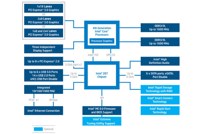
Lynx Point[edit]
Lynx Point is the codename of a PCH in Intel 8 Series chipsets, most closely associated with Haswell processors with LGA 1150 socket.[10] The Lynx Point chipset connects to the processor primarily over the Direct Media Interface (DMI) interface.[11]
The following variants are available:[12]
- DH82C222 (PCH C222) Workstation/Server
- DH82C224 (PCH C224) Workstation/Server
- DH82C226 (PCH C226) Workstation/Server
- DH82H87 (PCH H87) Desktop Home
- DH82Z87 (PCH Z87) Combined desktop base and home
- DH82B85 (PCH B85) Desktop Office
- DH82Q87 (PCH Q87) Desktop Office
- DH82Q85 (PCH Q85) Desktop Office
- DH82HM87 (PCH HM87) Mobile Home
- DH82HM86 (PCH HM86) Mobile Home
- DH82QM87 (PCH QM87) Mobile Office
Issues[edit]
A design flaw causes devices connected to the Lynx Point's integrated USB 3.0 controller to be disconnected when the system wakes up from the S3 state (Suspend to RAM), forcing the USB devices to be reconnected although no data is lost.[13][14] This issue is corrected in C2 stepping level of the Lynx Point chipset.[15]
Wellsburg[edit]
Wellsburg is the codename of a future PCH most closely associated with Haswell-E and the Grantley platform. It replaces Patsburg and is based on Lynx Point.[16][17]
http://en.wikipedia.org/wiki/I/O_Controller_Hub
I/O Controller Hub
I/O Controller Hub (ICH) is a family of Intel southbridge microchips used to manage data communications between a CPU and a motherboard, specifically Intel chipsets based on the Intel Hub Architecture. It is designed to be paired with a second support chip known as anorthbridge. As with any other southbridge, the ICH is used to connect and control peripheral devices.
As CPU speeds increased data transmission between the CPU and support chipset eventually emerged as a bottleneck between the processor and the motherboard. Accordingly starting with the Intel 5 Series, a new architecture was used that incorporated some functions of the traditional north and south bridge chips onto the CPU itself, with the remaining functions being consolidated into a single Platform Controller Hub (PCH). This replaces the traditional two chip setup.
ICH[edit]
The first version of the ICH was released in June 1999 along with the Intel 810 northbridge. While its predecessor, the PIIX, was connected to the northbridge through an internal PCIbus with 133 MB/s, the ICH used a proprietary interface (called by Intel Hub Interface) that linked it to the northbridge through an 8-bit wide, 266 MB/s bus.
The Hub Interface was a point-to-point connection between different components on the motherboard. Another design decision was to substitute the rigid North-South axis on the motherboard with a star structure.
Note that, along with the ICH, Intel evolved other uses of the "Hub" terminology. Thus, the northbridge became the Memory Controller Hub (MCH) or if it had integrated graphics (e.g.,Intel 810), the Graphics and Memory Controller Hub (GMCH).
Other ICH features include:
- PCI Rev 2.2 compliant with support for 33 MHz PCI operations.
- Advanced Configuration and Power Interface (ACPI) Support
- Integrated IDE controller for Ultra ATA support
- Integrated I/O APIC supporting 24 interrupt sources
- System Management Bus (SMBus) with support for I²C devices
- AC'97 2.1 Compliant Link
- Low Pin Count (LPC) interface
The ICH came in two flavors:
- 82801AA (ICH) - Ultra ATA/66 support, 6 PCI slots, Alert on LAN support
- 82801AB (ICH0) - Ultra ATA/33 support, 4 PCI slots, no Alert on LAN
ICH2[edit]

In early 2000 Intel had suffered a significant setback with the i820 northbridge. Customers were not willing to pay the high prices for RDRAM and either bought i810 or i440BX motherboards or changed to the competition. The hastily developed 82815 northbridge for PC-133 SDRAM became Intel's method to recover in the middle class segment.
The ICH1 or the new ICH2 (360 pins) could be placed to the side of the 82815. An ICH2 could also be used with Intel's 82850 chipset, which, like the 82820 before it, required the use of RDRAM and supported the Pentium 4 CPU. For the first time a Fast Ethernet chip (82559) was integrated into the southbridge, depending upon an external PHY chip.
The PATA interface was accelerated to ATA/100 and the number of USB connections was doubled to four. The integrated AC'97 sound controller gained support for up to six channel sound....
There was also a mobile variant called the ICH2-M.
The following variants existed:
- 82801BA (ICH2)
- 82801BAM (ICH2-M) Mobile
ICH3[edit]
In 2001, Intel delivered ICH3, which was available in two versions: the server version, ICH3-S, running with the E7501 Northbridge, and the mobile version, ICH3-M, which worked with the i830 and i845 northbridges. There is no version for desktop motherboards.
In comparison with the ICH2, the changes were limited: "Native Mode" support in the PATA Controller; up to six USB-1.1 devices; SMBus 2.0; and the newest SpeedStep version, which allowed power-saving devices to be switched off during operation. The chip had 421 pins.
This has the following variants:
- 82801CA (ICH3-S) Server
- 82801CAM (ICH3-M) Mobile
ICH4[edit]

The ICH4 was Intel's southbridge for the year 2002. The most important innovation was the support of USB 2.0 on all six ports. Sound support was improved and corresponded the newest AC'97 specification, version 2.3. Like the preceding generation, the ICH4 had 421 pins.
This has the following variants:
ICH5[edit]

In 2003, and in conjunction with the i865 and i875 northbridges, the ICH5 was created. A SATA host controller was integrated. The ICH5R variant additionally supported RAID 0 on SATA ports. Eight USB-2.0 ports were available. The chip had full support for ACPI 2.0. It had 460 pins.
Since 1999 the 266 MB/s hub interface was assumed to be a bottleneck. In the new chip generation, Intel therefore offered an optional port for a Gigabit Ethernet Controller directly attached to the MCH.
The goal of this CSA technology was to reduce the latencies for Gigabit LAN by direct memory access and to free up bandwidth on the Hub interface between ICH and MCH for non removable disk and PCI data traffic.
Since mid-2004, the large motherboard manufacturers noticed an increased complaint ratio with motherboards equipped with ICH5. A cause was the insufficient ESD tolerance of certain ICH5 steppings.
In particular, when connecting USB devices via front panels, the chips died by discharges of static electricity. Intel reacted to the problem by shipping ICH5 with increased ESD tolerance. Effective ESD preventive measures on USB ports are difficult and costly, since they can impair signal quality of the USB-2.0 high-speed signals. Many motherboard manufacturers had omitted the necessary high-quality safety devices for front panel connectors for cost reasons.
This has the following variants:
- 82801E (C-ICH) Communications
- 82801EB (ICH5) Base
- 82801ER (ICH5R) RAID
- 82801EBM (ICH5-M) Base Mobile
- 6300ESB (ESB) Enterprise Southbridge
ICH6[edit]

ICH6 was Intel's first PCI Express southbridge. It made four PCI Express ×1 ports available. Faster ×16-Ports were accommodated in the MCH. The bottleneck Hub interface was replaced by a new Direct Media Interface (in reality a PCI Express ×4 link) with 1 GB/s per direction. Support for Intel High Definition Audio was included. In addition, AC'97and the classical PCI 2.3 were still supported.
Two additional SATA ports were added, and one PATA channel was removed. The ICH6R variant supported RAID modes 0, 1, 0+1 and the Intel specific "Matrix RAID".
ICH6R and ICH6-M implemented AHCI SATA controllers for the first time. The chips had 652 pins. Originally Intel had planned to bring two further variants under the names ICH6W and ICH6RW to the market, which should contain a software Access Point for a Wireless LAN. These chips are published.
This has the following variants:
- 82801FB (ICH6) Base
- 82801FR (ICH6R) RAID
- 82801FBM (ICH6M) Base Mobile
- 6311ESB (ESB2) Enterprise Southbridge
- 6321ESB (ESB2) Enterprise Southbridge with integrated LAN for embedded
ICH7[edit]
_on_motherboard.jpg)
The ICH7 started to ship in mid-2005 together with Intel's new high-end MCH, the i955X. Two additional PCI express ×1-Ports, an accelerated SATA Controller for up to 300 MB/s data transmission rate (the mobile version has this capability disabled), as well as support for Intel's "Active Management Technology" were added. Only the ICH7DH, ICH7R, ICH7-M, ICH7-M DH chip have AHCI support. The ICH7 (Base) and ICH7-U (Ultra-mobile) chip do not support AHCI.
The ICH7R additionally supports RAID 5.
This has the following variants:
- 82801GB (ICH7) Base
- 82801GR (ICH7R) RAID
- 82801GDH (ICH7DH) Digital Home
- 82801GBM (ICH7M) Mobile
- 82801GHM (ICH7M DH) Mobile Digital Home
- PC82801GU (ICH7-U) Ultra-mobile
ICH8[edit]
ICH8 is offered in several different versions and is the complement to the 965 class MCH chips. The non-mobile ICH8 does not have a traditional PATA interface, and just one AC'97. In practice, most baseboard manufacturers still offered PATA appropriate connection types using additional chips from manufacturers such as JMicron or Marvell.
The ICH8 was the first ICH model to control eSATA and Gigabit Ethernet, which were previously accommodated in the MCH. The base version only includes four SATA 2.0 ports.
The ICH8R (RAID) and above chips support six SATA devices. Additionally the ICH8DH (Digital Home) has Quick Resume and can be used together with the P965 and/or G965 in Intel Viiv-certified systems.
The counterpart to the ICH8DO (Digital Office) is the Q965 MCH, which together provide Intel vPro compatibility.
This has the following variants:
- 82801HB (ICH8) Base
- 82801HR (ICH8R) RAID
- 82801HH (ICH8DH) Digital Home
- 82801HO (ICH8DO) Digital Office
- 82801HM (ICH8M) Mobile
- 82801HEM (ICH8EM) Enhanced Mobile
ICH9[edit]
The ICH9 came out in May 2007 in the P35 (Bearlake) chipset. It removes all PATA support. In practice, many baseboard manufacturers continue providing PATA using an additional chip. Officially only the ICH9R, ICH9DH, ICH9DO chip have AHCI support.
This part has the following variants:
- 82801IB (ICH9) Base officially neither AHCI or RAID support, but a simple driver INF edit shows it supports AHCI without problems[citation needed]
- 82801IR (ICH9R) RAID with AHCI and RAID Support
- 82801IH (ICH9DH) Digital Home with AHCI and no RAID Support
- 82801IO (ICH9DO) Digital Office with AHCI and RAID Support
- 82801IBM (ICH9M) Base Mobile
- 82801IEM (ICH9EM) Enhanced Mobile
- 82801IUX (ICH9M-SFF) Ultra Mobile
ICH10[edit]
Intel launched the ICH10 southbridge in June 2008 with the P45 (Eaglelake) chipset.
ICH10 implements the 10Gbit/s bidirectional DMI interface to the "northbridge" device. It supports various interfaces to "low-speed" peripherals, and it supports a suite of housekeeping functions.
ICH10 also offers reduced load on CPU and decreased power consumption.
ICH10 does not offer direct PATA or LPT support. Notably there is support of 'hot-swap' functionality.
The RAID variant also supports a new technology called “Turbo Memory”. This allows the use of flash memory on a motherboard for fast caching.
Peripheral support includes:
- Six PCIe version 1.1 ports, four of which can be configured as either 4 ×1 or 1 ×4.
- PCI bus
- Six SATA 3 Gbit/s ports in either legacy IDE or AHCI mode. Can support external eSATA
- Intel High Definition Audio
- Integrated gigabit LAN.
- Two EHCI host controllers (which support up to twelve USB 2.0 connections)
This part has the following variants:
- 82801JB (ICH10) Base
- 82801JR (ICH10R) RAID
- 82801JH (ICH10D) Digital Home
- 82801JO (ICH10DO) Digital Office
PCH architecture[edit]
As CPU speeds increased a bottleneck eventually emerged between the processor and the motherboard, due to limitations caused by data transmission between the CPU and southbridge. Accordingly starting with the Intel 5 Series, a new architecture was used where some functions of the north and south bridge chips were moved to the CPU, and others were consolidated into a Platform Controller Hub(PCH).
- Some northbridge functions, including the memory controller and Graphics (PCI-e) lanes, were integrated into the CPU while the PCH took over the remaining functions in addition to the traditional roles of the southbridge. The northbridge was therefore eliminated.
- Other northbridge functions and all southbridge functions were migrated to a new Platform Controller Hub. These included clocking (the system clock), Flexible Display Interface (FDI) and Direct Media Interface (DMI). The FDI is only used when the chipset requires supporting a processor with integrated graphics.
http://en.wikipedia.org/wiki/Intel_X58
I/O Hub, an Intel chipset architecture
Intel X58
| Codename(s) | Tylersburg |
|---|---|
| CPU supported | |
| Socket supported | LGA 1366 |
| Fabrication process | 65 nm |
| Southbridge(s) | ICH10 |
| Miscellaneous | |
| Release date(s) | November 2008 |
| Predecessor |
|
| Successor | Intel X79 (Patsburg PCH) |

The Intel X58 (codenamed Tylersburg) is an Intel chip designed to connect Intel processors with Intel QuickPath Interconnect (QPI) interface to peripheral devices. Supported processors implement the Nehalem microarchitecture and therefore have an integrated memory controller (IMC), so the X58 does not have a memory interface. Initially supported processors were the Core i7,[1] but the chip also supported Nehalem-based Xeon processors.
Description[edit]
The QuickPath architecture differs considerably from earlier Intel architectures, and is much closer to AMD's HyperTransport architecture. Except for the lack of a memory interface, the X58 is similar to the traditional northbridge: it communicates with the processor(s) via the high bandwidth QuickPath Interconnect, it communicates with the southbridge via Direct Media Interface (DMI), and it communicates with high bandwidth peripherals via PCI Express (PCIe).
The X58 is not a memory controller hub (MCH), because it has no memory interface, so Intel calls it an I/O hub. This should not be confused with the similar termI/O controller hub (ICH) which has traditionally been used to refer to the southbridge chips. Intel documentation now refers to the southbridge as the Legacy I/O Controller Hub.
The X58 has 40 PCIe lanes that are arranged in two ×16 links, DMI link and "spare"-based link. When used with the ICH10 I/O Controller Hub with ×4 DMI connection the "spare" supports a separate ×4 PCIe connection. Future southbridge chips DMI may support a wider DMI.
Each X58 QuickPath Interconnect uses 21 unidirectional differential pairs in each direction, for a total of 84 pins per QPI. At the highest bandwidth, each QPI can transfer up to 12.8 GB/s usable in each direction simultaneously using the QPI protocol. The protocol transfers information in units of 80 bits (called "flits") which contain 8 bits of error correction, 8 bits of QPI routing information, and 64 bits of data.
X58 PCIe ports support full PCIe 2.0 bandwidth (e.g., up to 8GB/s per ×16 link) and each ×16 link may be divided into total 16 lanes in any combination of ×8, ×4, ×2 or ×1 ports. They also support all features of line-reserved wiring, which means that in the combinations of (×16 + ×1/×8) slots, often used on the motherboards, not only ×1 or ×8 cards may be installed into the ×1/×8 slot, but ×4 cards should work as well (if not disallowed by the motherboard BIOS.)
Unlike the front-side bus (FSB), QPI is a point-to-point interface and supports not only processor-chipset interface, but also processor-to-processor connection and chip-to-chip connection. The X58 has two QPIs and can directly connect to two processors on a multi-socket motherboard or form a ring-like connection (processor 1 to X58 to processor 2 back to processor 1). When used with the Intel Core i7, the second QPI is usually unused (though, in principle, the second X58 might be daisy-chained on the board).
When used with the "Gainestown" DP processor, which will have two QPIs, the X58 and the two processors may be connected in a triangle or ring. For MP processors such as "Beckton" with more than two QPIs, the X58 is either connected to two processors, which in turn are connected in a "mesh" of QPIs to other processors or attached "in pairs" to two different processors. I/O for "remote" processors is relayed via the inter-processors QPI.
X58 board manufacturers can build SLI-compatible Intel chipset boards by submitting their designs to nVidia for validation. However, users wishing to run more than two Nvidia video cards in PCIe ×16 will still need to purchase motherboards equipped with one or more nVidia nForce chipsets. It is still possible to run more than two video cards in an SLI-configuration at fewer PCIe lane widths.[2] The X58 chipset itself supports up to 36 PCI-Express 2.0 lanes, so it is possible to have two PCIe ×16 slots and one PCIe ×4 slot on the same motherboard.[1]
Interfaces[edit]
- QPI (Intel QuickPath Interconnect)[3]
- PCI Express 2.0
- ICH10-compatible DMI.
See also[edit]
http://en.wikipedia.org/wiki/System_Controller_Hub
System Controller Hub
System Controller Hub (SCH) is a family of Intel microchips employed in chipsets for low-power Atom-based platforms. Its architecture is consistent with the Intel Hub Architecture but combines the traditional northbridge and southbridge functions into a single microchip.
Poulsbo[edit]
Poulsbo is the codename of the first SCH and plays a key role in Intel's second-generation Menlow UMPC and MID platform chipset for Atom Silverthornemicroprocessors.[1][2]
The graphics core is called GMA 500 and unlike most graphics cores used by Intel was developed by Imagination Technologies. Intel licensed the PowerVR SGX 535 as a graphics core and the PowerVR VXD370 for H.264/MPEG-4 AVC playback. The video core is able to process 720p as well as 1080i resolutions.[3]
This has the following variations:[4]
GMA 500 Linux support[edit]
Although several netbooks using the Poulsbo chipset are shipped with some distribution of Linux (notably the Sony Vaio P and Dell Inspiron Mini 12, among others), Poulsbo's graphics core GMA 500 is currently not well supported by Intel for Linux.
A proprietary driver was shipped with Dell's adaptation of Ubuntu 8.04.1 Netbook Remix, which provides 2D hardware acceleration (although users reported serious stability issues[5]) under Linux kernel 2.6.24. A work-in-progress free driver is currently available, however the proprietary driver does not work with current Linux kernels and current versions of X.[6] Work is under way to provide at least 2D support in current Linux kernels,[7] although this will still rely on proprietary binary code for the 3D part of the driver. The current[8] status of this driver runs on Fedora 10 and allows for 2D. 3D acceleration, however, is still broken.
A working, proprietary driver package is available for Fedora 11.[9]
Starting with Mandriva 2010 Release Candidate 2, Poulsbo drivers are now fully supported out of the box when you use One isos. Hardware will be automatically detected and configured using XFdrake. As it needs non-free firmware, this could not be included in Free isos.[10]
A rudimentary (no 3D acceleration) driver was added to Linux 2.6.39.[11][12]
Whitmore Lake[edit]
Whitmore Lake is the codename of another SCH.
This has the following variations:[13]