开发环境:win10 64位 + VMware12 + Ubuntu14.04 32位
工具链:linaro提供的gcc-linaro-6.1.1-2016.08-x86_64_arm-linux-gnueabi
要移植的u-boot版本:u-boot-2016-11
Tiny4412开发板硬件版本为:
底板: Tiny4412SDK 1312B
核心板:Tiny4412 - 1306
----------------------------------------------------------------------------------------------------------------------------------------------
2019.02.04 第二次修改:
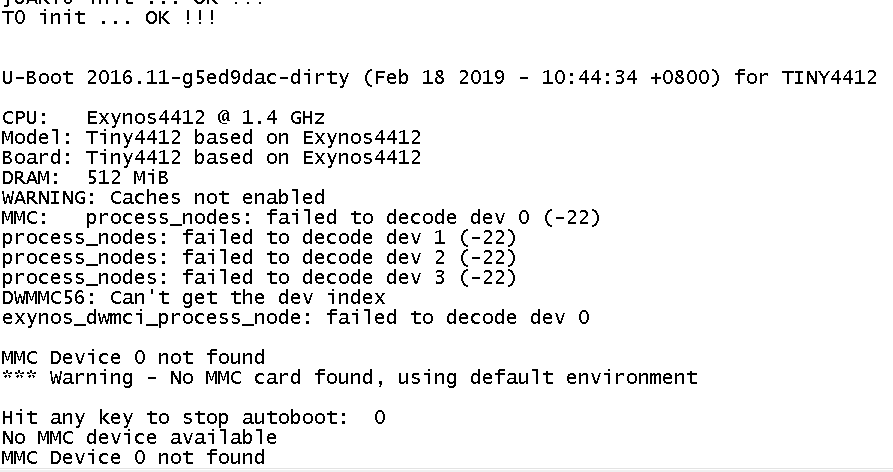
原因:Uboot启动后DRAM显示错误;
diff --git a/arch/arm/mach-exynos/dmc_init_exynos4412.c b/arch/arm/mach-exynos/d
index f096f25..2b2bc3b 100644
--- a/arch/arm/mach-exynos/dmc_init_exynos4412.c
+++ b/arch/arm/mach-exynos/dmc_init_exynos4412.c

 struct mem_timings mem = {
    .direct_cmd_msr = {
        DIRECT_CMD1, DIRECT_CMD2, DIRECT_CMD3, DIRECT_CMD4
@@ -179,7 +180,6 @@ static void dmc_init(struct exynos4_dmc *dmc)
    writel(DIRECT_CMD_ZQ, &dmc->directcmd);
    sdelay(0x100000);

-#ifndef TINY4412
    /* Chip1: NOP Command: Assert and Hold CKE to high level */
    writel((DIRECT_CMD_NOP | DIRECT_CMD_CHIP1_SHIFT), &dmc->directcmd);
    sdelay(0x100000);
@@ -191,7 +191,6 @@ static void dmc_init(struct exynos4_dmc *dmc)
    /* Chip1: ZQINIT */
    writel((DIRECT_CMD_ZQ | DIRECT_CMD_CHIP1_SHIFT), &dmc->directcmd);
    sdelay(0x100000);
-#endif

    phy_control_reset(1, dmc);
    sdelay(0x100000);
diff --git a/include/configs/tiny4412.h b/include/configs/tiny4412.h
index 197fd14..08fb652 100644
--- a/include/configs/tiny4412.h
+++ b/include/configs/tiny4412.h

/* High Level Configuration Options */
 #define TINY4412         1
@@ -21,26 +18,30 @@
 #define CONFIG_SYS_DCACHE_OFF          1

 /* TINY4412 has 8 bank of DRAM */
-#define CONFIG_NR_DRAM_BANKS           8
+#define CONFIG_NR_DRAM_BANKS           4
 #define CONFIG_SYS_SDRAM_BASE          0x40000000
 #define PHYS_SDRAM_1                   CONFIG_SYS_SDRAM_BASE
-#define SDRAM_BANK_SIZE                        (128 << 20)     /* 128 MB */
+#define SDRAM_BANK_SIZE                            0x10000000   /*(256 << 20)

 /* memtest works on */
 #define CONFIG_SYS_MEMTEST_START       CONFIG_SYS_SDRAM_BASE
-#define CONFIG_SYS_MEMTEST_END         (CONFIG_SYS_SDRAM_BASE + 0x6000000)
-#define CONFIG_SYS_LOAD_ADDR           (CONFIG_SYS_SDRAM_BASE + 0x3E00000)
+#define CONFIG_SYS_MEMTEST_END         (CONFIG_SYS_SDRAM_BASE + 0x5e00000)
+#define CONFIG_SYS_LOAD_ADDR           (CONFIG_SYS_SDRAM_BASE + 0x3e00000)
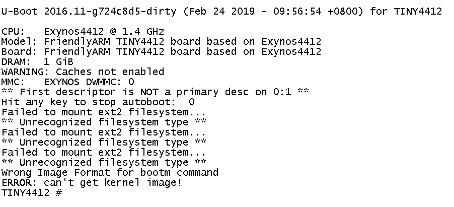
但是启动的ext2格式还是有问题,目前还在解决当中。
——————————————————————————————————————————————————————————————————————
上述问题已解决:tiny4412 --Uboot移植(6) SD卡驱动,启动内核
1、原理图
Exynos4412中有两个独立的DRAM控制器,分别叫DMC0和DMC1。DMC0和DMC1分别支持最大1.5GB的DRAM,它们都支持DDR2/DDR3和LPDDR2等,512 Mb, 1 Gb, 2 Gb, 4 Gb and 8 Gbit的内存设备,支持16/32bit的位宽。DRAM0 对应的地址是0x4000_0000~0xAFFF_FFF共1.5GB,DRAM1 对应的地址是0xA000_000~0x0000_0000共1.5GB。

Tiny4412的1GB的DRAM是由4片大小为128MX16的DDR3芯片组合而成,下面看一下Tiny4412的原理图
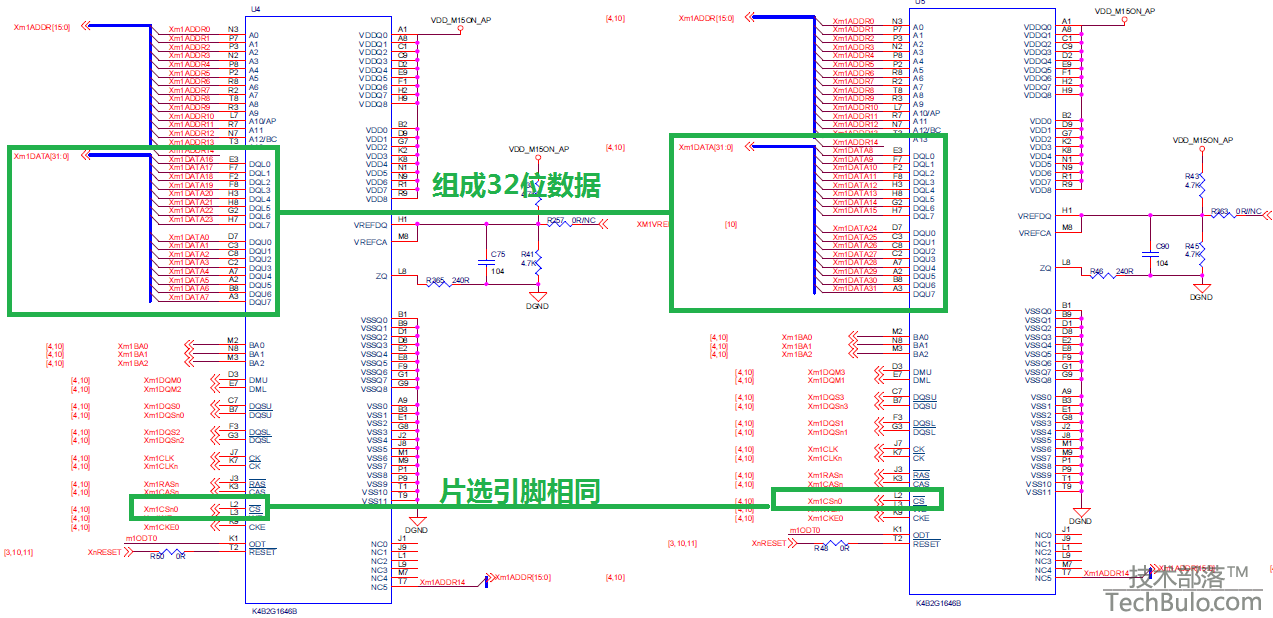
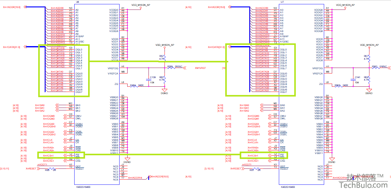
从上两图可以看出,这四片DDR 芯片被分成了两两一组,组成32位数据,四片都是挂接到DMC0处。
2,DDR3初始化代码
diff --git a/arch/arm/mach-exynos/Makefile b/arch/arm/mach-exynos/Makefil
index 5575adf..5889802 100644
--- a/arch/arm/mach-exynos/Makefile
+++ b/arch/arm/mach-exynos/Makefile
@@ -15,7 +15,7 @@ ifdef CONFIG_SPL_BUILD
 obj-$(CONFIG_EXYNOS5)  += clock_init_exynos5.o
 obj-$(CONFIG_EXYNOS5)  += dmc_common.o dmc_init_ddr3.o
 obj-$(CONFIG_EXYNOS4210)+= dmc_init_exynos4.o clock_init_exynos4.o
-obj-$(CONFIG_EXYNOS4412)+= dmc_init_exynos4.o clock_init_exynos4412.o
+obj-$(CONFIG_EXYNOS4412)+= dmc_init_exynos4412.o clock_init_exynos4412.o

 obj-y  += spl_boot.o tzpc.o
 obj-y  += lowlevel_init.o
diff --git a/arch/arm/mach-exynos/dmc_init_exynos4412.c b/arch/arm/mach-e
new file mode 100644
index 0000000..b2c0c0d
--- /dev/null
+++ b/arch/arm/mach-exynos/dmc_init_exynos4412.c
@@ -0,0 +1,254 @@
+/*
+ * Memory setup for board based on EXYNOS4412
+ *
+ *                 2016
+ * Modified by AP0904225 <ap0904225@qq.com>
+ *
+ * Copyright (C) 2013 Samsung Electronics
+ * Rajeshwari Shinde <rajeshwari.s@samsung.com>
+ *
+ * See file CREDITS for list of people who contributed to this
+ * project.
+ *
+ * This program is free software; you can redistribute it and/or
+ * modify it under the terms of the GNU General Public License as
+ * published by the Free Software Foundation; either version 2 of
+ * the License, or (at your option) any later version.
+ *
+ * This program is distributed in the hope that it will be useful,
+ * but WITHOUT ANY WARRANTY; without even the implied warranty of
+ * MERCHANTABILITY or FITNESS FOR A PARTICULAR PURPOSE.  See the
+ * GNU General Public License for more details.
+ *
+ * You should have received a copy of the GNU General Public License
+ * along with this program; if not, write to the Free Software
+ * Foundation, Inc., 59 Temple Place, Suite 330, Boston,
+ * MA 02111-1307 USA
+ */++#include <config.h>+#include <asm/arch/dmc.h>+#include "common_setup.h"+#include "exynos4412_setup.h"++#ifdef TINY4412
+struct mem_timings mem = {
+   .direct_cmd_msr = {
+       DIRECT_CMD1, DIRECT_CMD2, DIRECT_CMD3, DIRECT_CMD4
+   .timingref = 0x000000BB,
+   .timingrow   = 0x4046654f,
+   .timingdata  = 0x46400506,
+   .timingpower = 0x52000A3C,
+   .zqcontrol   = 0xE3854C03,
+   .control0    = 0x71101008,
+   .control1    = 0xe0000086,
+   .control2    = 0x00000000,
+   .concontrol  = 0x0FFF301A,
+   .prechconfig = 0xff000000,
+   .memcontrol  = 0x00312640,      /* Tiny4412-1306 core board  use chip0/1 */
+   .memconfig0  = 0x40e01323,      /* ROW is 15bit */
+   .memconfig1  = 0x60e01323,      /* DMC0 address up to 0xfFFFFFFF */
+   .dll_resync  = FORCE_DLL_RESYNC,
+   .dll_on      = DLL_CONTROL_ON,
+
+};
+#else
+struct mem_timings mem = {+   .direct_cmd_msr = {+       DIRECT_CMD1, DIRECT_CMD2, DIRECT_CMD3, DIRECT_CMD4+   },+   .timingref = TIMINGREF_VAL,+   .timingrow = TIMINGROW_VAL,+   .timingdata = TIMINGDATA_VAL,+   .timingpower = TIMINGPOWER_VAL,+   .zqcontrol = ZQ_CONTROL_VAL,+   .control0 = CONTROL0_VAL,+   .control1 = CONTROL1_VAL,+   .control2 = CONTROL2_VAL,+   .concontrol = CONCONTROL_VAL,+   .prechconfig = PRECHCONFIG,+   .memcontrol = MEMCONTROL_VAL,+   .memconfig0 = MEMCONFIG0_VAL,+   .memconfig1 = MEMCONFIG1_VAL,+   .dll_resync = FORCE_DLL_RESYNC,+   .dll_on = DLL_CONTROL_ON,+};+#endif
++static void phy_control_reset(int ctrl_no, struct exynos4_dmc *dmc)+{+   if (ctrl_no) {+       writel((mem.control1 | (1 << mem.dll_resync)),+              &dmc->phycontrol1);+       writel((mem.control1 | (0 << mem.dll_resync)),+              &dmc->phycontrol1);+   } else {+       writel((mem.control0 | (0 << mem.dll_on)),+              &dmc->phycontrol0);+       writel((mem.control0 | (1 << mem.dll_on)),+              &dmc->phycontrol0);+   }+}++static void dmc_config_mrs(struct exynos4_dmc *dmc, int chip)+{+   int i;+   unsigned long mask = 0;++   if (chip)+       mask = DIRECT_CMD_CHIP1_SHIFT;++   for (i = 0; i < MEM_TIMINGS_MSR_COUNT; i++) {+       writel(mem.direct_cmd_msr[i] | mask,+              &dmc->directcmd);+   }+}++static void dmc_init(struct exynos4_dmc *dmc)+{+   /*
+    * DLL Parameter Setting:
+    * Termination: Enable R/W
+    * Phase Delay for DQS Cleaning: 180' Shift
+    */+   writel(mem.control1, &dmc->phycontrol1);++   /*
+    * ZQ Calibration
+    * Termination: Disable
+    * Auto Calibration Start: Enable
+    */+   writel(mem.zqcontrol, &dmc->phyzqcontrol);+   sdelay(0x100000);++   /*
+    * Update DLL Information:
+    * Force DLL Resyncronization
+    */+   phy_control_reset(1, dmc);+   phy_control_reset(0, dmc);++   /* Set DLL Parameters */+   writel(mem.control1, &dmc->phycontrol1);++   /* DLL Start */+   writel((mem.control0 | CTRL_START | CTRL_DLL_ON), &dmc->phycontrol0);
++   writel(mem.control2, &dmc->phycontrol2);++   /* Set Clock Ratio of Bus clock to Memory Clock */+   writel(mem.concontrol, &dmc->concontrol);++   /*
+    * Memor Burst length: 8
+    * Number of chips: 2
+    * Memory Bus  32 bit
+    * Memory Type: DDR3
+    * Additional Latancy for PLL: 1 Cycle
+    */+   writel(mem.memcontrol, &dmc->memcontrol);++   writel(mem.memconfig0, &dmc->memconfig0);+   writel(mem.memconfig1, &dmc->memconfig1);+
+#ifdef TINY4412
+   writel(0x8000001F, &dmc->ivcontrol);
+#endif
++   /* Config Precharge Policy */+   writel(mem.prechconfig, &dmc->prechconfig);+   /*
+    * TimingAref, TimingRow, TimingData, TimingPower Setting:
+    * Values as per Memory AC Parameters
+    */+   writel(mem.timingref, &dmc->timingref);+   writel(mem.timingrow, &dmc->timingrow);+   writel(mem.timingdata, &dmc->timingdata);+   writel(mem.timingpower, &dmc->timingpower);++   /* Chip0: NOP Command: Assert and Hold CKE to high level */+   writel(DIRECT_CMD_NOP, &dmc->directcmd);+   sdelay(0x100000);++   /* Chip0: EMRS2, EMRS3, EMRS, MRS Commands Using Direct Command */+   dmc_config_mrs(dmc, 0);+   sdelay(0x100000);++   /* Chip0: ZQINIT */+   writel(DIRECT_CMD_ZQ, &dmc->directcmd);+   sdelay(0x100000);++//#ifndef TINY4412
+   /* Chip1: NOP Command: Assert and Hold CKE to high level */+   writel((DIRECT_CMD_NOP | DIRECT_CMD_CHIP1_SHIFT), &dmc->directcmd);+   sdelay(0x100000);++   /* Chip1: EMRS2, EMRS3, EMRS, MRS Commands Using Direct Command */+   dmc_config_mrs(dmc, 1);+   sdelay(0x100000);++   /* Chip1: ZQINIT */+   writel((DIRECT_CMD_ZQ | DIRECT_CMD_CHIP1_SHIFT), &dmc->directcmd);+   sdelay(0x100000);+//#endif
++   phy_control_reset(1, dmc);+   sdelay(0x100000);++   /* turn on DREX0, DREX1 */+   writel((mem.concontrol | AREF_EN), &dmc->concontrol);+}++void mem_ctrl_init(int reset)+{+   struct exynos4_dmc *dmc;++   /*
+    * Async bridge configuration at CPU_core:
+    * 1: half_sync
+    * 0: full_sync
+    */+   writel(1, ASYNC_CONFIG);++#ifndef TINY4412+#ifdef CONFIG_ORIGE+   /* Interleave: 2Bit, Interleave_bit1: 0x15, Interleave_bit0: 0x7 */+   writel(APB_SFR_INTERLEAVE_CONF_VAL, EXYNOS4_MIU_BASE +       APB_SFR_INTERLEAVE_CONF_OFFSET);+   /* Update MIU Configuration */+   writel(APB_SFR_ARBRITATION_CONF_VAL, EXYNOS4_MIU_BASE +       APB_SFR_ARBRITATION_CONF_OFFSET);+#else
+   writel(APB_SFR_INTERLEAVE_CONF_VAL, EXYNOS4_MIU_BASE +       APB_SFR_INTERLEAVE_CONF_OFFSET);+   writel(INTERLEAVE_ADDR_MAP_START_ADDR, EXYNOS4_MIU_BASE +       ABP_SFR_INTERLEAVE_ADDRMAP_START_OFFSET);+   writel(INTERLEAVE_ADDR_MAP_END_ADDR, EXYNOS4_MIU_BASE +       ABP_SFR_INTERLEAVE_ADDRMAP_END_OFFSET);+   writel(INTERLEAVE_ADDR_MAP_EN, EXYNOS4_MIU_BASE +       ABP_SFR_SLV_ADDRMAP_CONF_OFFSET);+#ifdef CONFIG_MIU_LINEAR+   writel(SLAVE0_SINGLE_ADDR_MAP_START_ADDR, EXYNOS4_MIU_BASE +       ABP_SFR_SLV0_SINGLE_ADDRMAP_START_OFFSET);+   writel(SLAVE0_SINGLE_ADDR_MAP_END_ADDR, EXYNOS4_MIU_BASE +       ABP_SFR_SLV0_SINGLE_ADDRMAP_END_OFFSET);+   writel(SLAVE1_SINGLE_ADDR_MAP_START_ADDR, EXYNOS4_MIU_BASE +       ABP_SFR_SLV1_SINGLE_ADDRMAP_START_OFFSET);+   writel(SLAVE1_SINGLE_ADDR_MAP_END_ADDR, EXYNOS4_MIU_BASE +       ABP_SFR_SLV1_SINGLE_ADDRMAP_END_OFFSET);+   writel(APB_SFR_SLV_ADDR_MAP_CONF_VAL, EXYNOS4_MIU_BASE +       ABP_SFR_SLV_ADDRMAP_CONF_OFFSET);+#endif
+#endif
+#endif
++   /* DREX0 */+   dmc = (struct exynos4_dmc *)samsung_get_base_dmc_ctrl();+   dmc_init(dmc);++   /* DREX1 */+   dmc = (struct exynos4_dmc *)(samsung_get_base_dmc_ctrl()+                +DMC_OFFSET);+   dmc_init(dmc);+}
diff --git a/arch/arm/mach-exynos/exynos4412_setup.h b/arch/arm/mach-exyn
index 11e9d09..fced9a8 100644
--- a/arch/arm/mach-exynos/exynos4412_setup.h
+++ b/arch/arm/mach-exynos/exynos4412_setup.h

+/* Bus Configuration Register Address */+#define ASYNC_CONFIG       0x10010350
++/* DMC */+#define DIRECT_CMD_NOP 0x07000000
+#define DIRECT_CMD_ZQ  0x0a000000
+#define DIRECT_CMD_CHIP1_SHIFT (1 << 20)
+#define MEM_TIMINGS_MSR_COUNT  4
+#define CTRL_START (1 << 0)
+#define CTRL_DLL_ON    (1 << 1)
+#define AREF_EN        (1 << 5)
+#define DRV_TYPE   (1 << 6)
++struct mem_timings {+   unsigned direct_cmd_msr[MEM_TIMINGS_MSR_COUNT];+   unsigned timingref;+   unsigned timingrow;+   unsigned timingdata;+   unsigned timingpower;+   unsigned zqcontrol;+   unsigned control0;+   unsigned control1;+   unsigned control2;+   unsigned concontrol;+   unsigned prechconfig;+   unsigned memcontrol;+   unsigned memconfig0;+   unsigned memconfig1;+   unsigned dll_resync;+   unsigned dll_on;+};++/* MIU */+/* MIU Config Register Offsets*/+#define APB_SFR_INTERLEAVE_CONF_OFFSET 0x400
+#define APB_SFR_ARBRITATION_CONF_OFFSET    0xC00
+#define ABP_SFR_SLV_ADDRMAP_CONF_OFFSET    0x800
+#define ABP_SFR_INTERLEAVE_ADDRMAP_START_OFFSET    0x808
+#define ABP_SFR_INTERLEAVE_ADDRMAP_END_OFFSET  0x810
+#define ABP_SFR_SLV0_SINGLE_ADDRMAP_START_OFFSET   0x818
+#define ABP_SFR_SLV0_SINGLE_ADDRMAP_END_OFFSET 0x820
+#define ABP_SFR_SLV1_SINGLE_ADDRMAP_START_OFFSET   0x828
+#define ABP_SFR_SLV1_SINGLE_ADDRMAP_END_OFFSET 0x830
+++#ifdef TINY4412+/* Interleave: 2Bit, Interleave_bit1: 0x15, Interleave_bit0: 0x7 */+#define APB_SFR_INTERLEAVE_CONF_VAL    0x20001507
+#define APB_SFR_ARBRITATION_CONF_VAL   0x00000001
+#endif
++#define INTERLEAVE_ADDR_MAP_START_ADDR 0x40000000
+#define INTERLEAVE_ADDR_MAP_END_ADDR   0xbfffffff
+#define INTERLEAVE_ADDR_MAP_EN     0x00000001
++#ifdef CONFIG_MIU_1BIT_INTERLEAVED+/* Interleave_bit0: 0xC*/+#define APB_SFR_INTERLEAVE_CONF_VAL    0x0000000c
+#endif
+#ifdef CONFIG_MIU_2BIT_INTERLEAVED+/* Interleave: 2Bit, Interleave_bit1: 0x15, Interleave_bit0: 0xc */+#define APB_SFR_INTERLEAVE_CONF_VAL    0x2000150c
+#endif
+#define SLAVE0_SINGLE_ADDR_MAP_START_ADDR  0x40000000
+#define SLAVE0_SINGLE_ADDR_MAP_END_ADDR        0x7fffffff
+#define SLAVE1_SINGLE_ADDR_MAP_START_ADDR  0x80000000
+#define SLAVE1_SINGLE_ADDR_MAP_END_ADDR        0xbfffffff
+/* Enable SME0 and SME1*/+#define APB_SFR_SLV_ADDR_MAP_CONF_VAL      0x00000006
++#define FORCE_DLL_RESYNC   3
+#define DLL_CONTROL_ON     1
++#define DIRECT_CMD1    0x00020000
+#define DIRECT_CMD2    0x00030000
+#define DIRECT_CMD3    0x00010002
+#define DIRECT_CMD4    0x00000328
++#define CTRL_ZQ_MODE_NOTERM    (0x1 << 0)
+#define CTRL_ZQ_START      (0x1 << 1)
+#define CTRL_ZQ_DIV        (0 << 4)
+#define CTRL_ZQ_MODE_DDS   (0x7 << 8)
+#define CTRL_ZQ_MODE_TERM  (0x2 << 11)
+#define CTRL_ZQ_FORCE_IMPN (0x5 << 14)
+#define CTRL_ZQ_FORCE_IMPP (0x6 << 17)
+#define CTRL_DCC       (0xE38 << 20)
+#define ZQ_CONTROL_VAL     (CTRL_ZQ_MODE_NOTERM | CTRL_ZQ_START
+               | CTRL_ZQ_DIV | CTRL_ZQ_MODE_DDS+               | CTRL_ZQ_MODE_TERM | CTRL_ZQ_FORCE_IMPN+               | CTRL_ZQ_FORCE_IMPP | CTRL_DCC)++#define ASYNC          (0 << 0)
+#define CLK_RATIO      (1 << 1)
+#define DIV_PIPE       (1 << 3)
+#define AWR_ON         (1 << 4)
+#define AREF_DISABLE       (0 << 5)
+#define DRV_TYPE_DISABLE   (0 << 6)
+#define CHIP0_NOT_EMPTY        (0 << 8)
+#define CHIP1_NOT_EMPTY        (0 << 9)
+#define DQ_SWAP_DISABLE        (0 << 10)
+#define QOS_FAST_DISABLE   (0 << 11)
+#define RD_FETCH       (0x3 << 12)
+#define TIMEOUT_LEVEL0     (0xFFF << 16)
+#define CONCONTROL_VAL     (ASYNC | CLK_RATIO | DIV_PIPE | AWR_ON
+               | AREF_DISABLE | DRV_TYPE_DISABLE+               | CHIP0_NOT_EMPTY | CHIP1_NOT_EMPTY+               | DQ_SWAP_DISABLE | QOS_FAST_DISABLE+               | RD_FETCH | TIMEOUT_LEVEL0)++#define CLK_STOP_DISABLE   (0 << 1)
+#define DPWRDN_DISABLE     (0 << 2)
+#define DPWRDN_TYPE        (0 << 3)
+#define TP_DISABLE     (0 << 4)
+#define DSREF_DIABLE       (0 << 5)
+#define ADD_LAT_PALL       (1 << 6)
+#define MEM_TYPE_DDR3      (0x6 << 8)
+#define MEM_WIDTH_32       (0x2 << 12)
+#define NUM_CHIP_2     (1 << 16)
+#define BL_8           (0x3 << 20)
+#define MEMCONTROL_VAL     (CLK_STOP_DISABLE | DPWRDN_DISABLE
+               | DPWRDN_TYPE | TP_DISABLE | DSREF_DIABLE+               | ADD_LAT_PALL | MEM_TYPE_DDR3 | MEM_WIDTH_32+               | NUM_CHIP_2 | BL_8)+++#define CHIP_BANK_8        (0x3 << 0)
+#define CHIP_ROW_14        (0x2 << 4)
+#define CHIP_COL_10        (0x3 << 8)
+#define CHIP_MAP_INTERLEAVED   (1 << 12)
+#define CHIP_MASK      (0xe0 << 16)
+#ifdef CONFIG_MIU_LINEAR+#define CHIP0_BASE     (0x40 << 24)
+#define CHIP1_BASE     (0x60 << 24)
+#else
+#define CHIP0_BASE     (0x20 << 24)
+#define CHIP1_BASE     (0x40 << 24)
+#endif
+#define MEMCONFIG0_VAL     (CHIP_BANK_8 | CHIP_ROW_14 | CHIP_COL_10
+               | CHIP_MAP_INTERLEAVED | CHIP_MASK | CHIP0_BASE)+#define MEMCONFIG1_VAL     (CHIP_BANK_8 | CHIP_ROW_14 | CHIP_COL_10
+               | CHIP_MAP_INTERLEAVED | CHIP_MASK | CHIP1_BASE)++#define TP_CNT         (0xff << 24)
+#define PRECHCONFIG        TP_CNT
++#define CTRL_OFF       (0 << 0)
+#define CTRL_DLL_OFF       (0 << 1)
+#define CTRL_HALF      (0 << 2)
+#define CTRL_DFDQS     (1 << 3)
+#define DQS_DELAY      (0 << 4)
+#define CTRL_START_POINT   (0x10 << 8)
+#define CTRL_INC       (0x10 << 16)
+#define CTRL_FORCE     (0x71 << 24)
+#define CONTROL0_VAL       (CTRL_OFF | CTRL_DLL_OFF | CTRL_HALF
+               | CTRL_DFDQS | DQS_DELAY | CTRL_START_POINT+               | CTRL_INC | CTRL_FORCE)++#define CTRL_SHIFTC        (0x6 << 0)
+#define CTRL_REF       (8 << 4)
+#define CTRL_SHGATE        (1 << 29)
+#define TERM_READ_EN       (1 << 30)
+#define TERM_WRITE_EN      (1 << 31)
+#define CONTROL1_VAL       (CTRL_SHIFTC | CTRL_REF | CTRL_SHGATE
+               | TERM_READ_EN | TERM_WRITE_EN)++#define CONTROL2_VAL       0x00000000
++#ifdef TINY4412+#define TIMINGREF_VAL      0x000000BB
+#define TIMINGROW_VAL      0x4046654f
+#define    TIMINGDATA_VAL      0x46400506
+#define    TIMINGPOWER_VAL     0x52000A3C
+#else
+#define TIMINGREF_VAL      0x000000BC
+#ifdef DRAM_CLK_330+#define TIMINGROW_VAL      0x3545548d
+#define    TIMINGDATA_VAL      0x45430506
+#define    TIMINGPOWER_VAL     0x4439033c
+#endif
+#ifdef DRAM_CLK_400+#define TIMINGROW_VAL      0x45430506
+#define    TIMINGDATA_VAL      0x56500506
+#define    TIMINGPOWER_VAL     0x5444033d
+#endif
+#endif
++++ #endif /*__EXYNOS4412_SETUP__ */
diff --git a/arch/arm/mach-exynos/lowlevel_init.c b/arch/arm/mach-exynos/
index c69be57..2963b9d 100644
--- a/arch/arm/mach-exynos/lowlevel_init.c
+++ b/arch/arm/mach-exynos/lowlevel_init.c
@@ -229,7 +229,34 @@ int do_lowlevel_init(void)
         printascii("UART0 init ... OK !!!

");
 #endif
                mem_ctrl_init(actions & DO_MEM_RESET);
-               tzpc_init();
+
+       writel(0x44444444, 0x40000000);
+       if(readl(0x40000000) == 0x44444444)
+       printascii("addriss is :0x40000000 ;value is 0x44444444... !!!

+
+       writel(0x55555555, 0x50000004);
+       if(readl(0x50000004) == 0x55555555)
+       printascii("addriss is :0x50000004 ;value is 0x55555555... !!!

+
+       writel(0x66666666, 0x60000000);
+       if(readl(0x60000000) == 0x66666666)
+       printascii("addriss is :0x60000000 ;value is 0x66666666... !!!

+
+       writel(0x77777777, 0x70000000);
+       if(readl(0x70000000) == 0x77777777)
+       printascii("addriss is :0x70000000 ;value is 0x77777777... !!!

+
+       writel(0x88888888, 0x70000001);
+       if(readl(0x70000001) == 0x88888888)
+       printascii("addriss is :0x70000001 ;value is 0x88888888... !!!

+
+       writel(0x88888888, 0x7000000f);
+       if(readl(0x7000000f) == 0x88888888)
+       printascii("addriss is :0x7000000f ;value is 0x88888888... !!!

+
+       #ifndef TINY4412
+       tzpc_init();
+       #endif
        }

        return actions & DO_WAKEUP;
diff --git a/include/configs/tiny4412.h b/include/configs/tiny4412.h
index fef910f..197fd14 100644
--- a/include/configs/tiny4412.h
+++ b/include/configs/tiny4412.h
@@ -20,11 +20,11 @@

 #define CONFIG_SYS_DCACHE_OFF          1

-/* ORIGEN has 4 bank of DRAM */
-#define CONFIG_NR_DRAM_BANKS           4
+/* TINY4412 has 8 bank of DRAM */
+#define CONFIG_NR_DRAM_BANKS           8
 #define CONFIG_SYS_SDRAM_BASE          0x40000000
 #define PHYS_SDRAM_1                   CONFIG_SYS_SDRAM_BASE
-#define SDRAM_BANK_SIZE                        (256 << 20)     /* 256 MB
+#define SDRAM_BANK_SIZE                        (128 << 20)     /* 128 MB
3、测试结果
UART0 init ... OK !!!
addriss is :0x40000000 ;value is 0x44444444... !!!
addriss is :0x50000004 ;value is 0x55555555... !!!
addriss is :0x60000000 ;value is 0x66666666... !!!
addriss is :0x70000000 ;value is 0x77777777... !!!
addriss is :0x70000001 ;value is 0x88888888... !!!
addriss is :0x7000000f ;value is 0x88888888... !!!
到这里,我们就完成了把u-boot.bin从SD卡拷贝到DDR内存中并在内存中执行u-boot。
u-boot可以在DDR内存执行后,我们转向使用printf函数来打印调试信息。因此可以把SPL阶段的调试串口关闭了:
diff --git a/configs/tiny4412_defconfig b/configs/tiny4412_defconfig
index 25c6bfb..f02edbe 100644
--- a/configs/tiny4412_defconfig
+++ b/configs/tiny4412_defconfig
@@ -40,11 +40,11 @@ CONFIG_OF_CONTROL=y

 #DEBUG UART
 #
-CONFIG_DEBUG_UART=y
-CONFIG_SPL_SERIAL_SUPPORT=y
-CONFIG_SPL_GPIO_SUPPORT=y
-CONFIG_DEBUG_UART_S5P=y
-CONFIG_DEBUG_UART_BASE=0x13800000
-CONFIG_DEBUG_UART_CLOCK=100000000
+#CONFIG_DEBUG_UART=y
+#CONFIG_SPL_SERIAL_SUPPORT=y
+#CONFIG_SPL_GPIO_SUPPORT=y
+#CONFIG_DEBUG_UART_S5P=y
+#CONFIG_DEBUG_UART_BASE=0x13800000
+#CONFIG_DEBUG_UART_CLOCK=100000000

 #
——————————————————————————————————————————————————————————————————————————————————
本来自己也是迷迷糊糊跟着 LoTGu 这位大佬的脚步在前进,前几篇也有一些磕磕绊绊,但都不是什么大的问题。直到这里,DDR3 由于使用的核心板版本不同,外接的DDR3的型号不同,导致拷贝过来之后也是不能达到预期的效果。然后就只能自己死磕,看芯片手册确实的由很大的帮助,上面的初始化流程都有。我主要用于查看上面程序中标红的配置数字,花费了两天时间,终于出了结果。但是我的DROM显示出来还是只有512M,(原本应该是1G)。目前没有好的解决方法,还不知道对后续有没有影响。这条路很辛苦,我很享受辛苦过后的喜悦感。一切都会好起来的呃。。
——————————————————————————————————————————————————————---——————————
感谢:
https://home.cnblogs.com/u/LoTGu/ (主要是跟着这位走)
Tiny4412裸机程序之代码在DDR SDRAM中运行 http://www.techbulo.com/1509.html
Tiny4412裸机程序之DDR3初始化流程 http://www.techbulo.com/1501.html
DDR3内存详解,存储器结构+时序+初始化过程 https://blog.csdn.net/a_chinese_man/article/details/73381338
tiny4412sdk-1506原生uboot卡死 http://www.cnblogs.com/kevinhwang/p/5617629.html
大水猫:https://me.csdn.net/sinat_20006769