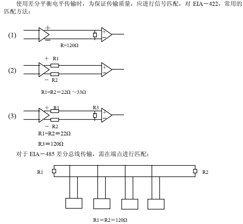
1、RS422/RS485
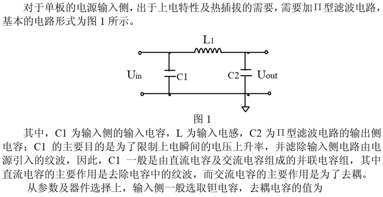
2、电源滤波
3、总线接口芯片选用具有三态输出功能的器件。
4、热插拔的模块要有加电保护器,GND--VCC--SIG的顺序上电。连接器的针脚长度不同,保证插拔时的通断顺序。
5、Altium Designer 封装库下载地址https://designcontent.live.altium.com/#UnifiedComponentDetail
6、Cadence17.2 PCB经常鼠标十字,无法操作----Win10自带输入法问题,卸载或者回退老版本解决。
7、PCB中慎用(那就不要用)负片,正片--所见即所得;负片--所见即为空。
8、Solder Mask层使用的是负片,所见即开窗(无绿油阻焊层)
9、磁珠使用注意:a、噪声频率;b、噪声需要衰减多少;c、负载阻抗;d、电流大小----注意DCR(直流电阻)。
10、耦合电容位置:1,按照design guideline 要求放置 2,没有guideline,如果是IC 到IC,请靠近接收端放置 3,如果是IC 到连接器,请靠近连接器放置 4,尽可能选择小的封装尺寸,减小阻抗不连续。---电容下面挖空,隔层参考(高频电路设计中,如何应对“不理想”的电容与电感? - 硬件 - EDA365电子论坛网)
11、FPGA高速通信接口供电电源芯片接地散热不理想,影响通信链路(PCIe)??
12、对外接口的接地影响实际波形(RS232,信号参考为经处理后的隔离地,实际对外接地为内部TTL地,对外通信乱码,自环可通。)