参考:http://www.cnblogs.com/zym0805/p/4815041.html
一. 硬件数据手册
The ST16C554D is a universal asynchronous receiver and transmitter (UART) with a dual foot print interface.
The 554D is an enhanced UART with 16 byte FIFOs, receive trigger levels and data rates up to 1.5Mbps.
The 554D is available in 64 pin TQFP, and 68 pin PLCC packages. The 68 pin PLCC package offer an additional 68 mode which allows easy integration with Motorola, and other popular microprocessors.
The 554D combines the package interface modes of the 16C554D and 68C554 series on a single integrated chip. The 16 mode interface is designed to operate with the Intel type of microprocessor bus while the 68 mode is intended to operate with Motorola, and other popular microprocessors. Following a reset, the 554D is down-ward compatible with the ST16C454/ST68C454 dependent on the state of the interface mode selection pin, 16/-68.
共有两种总线接口:16mode(Intel)和68mode(Motorola),板卡上用用ST16C554DIQ64,仅支持16mode。
PIN介绍
A0/A1/A2: Address-0/1/2 Select Bit. Internal registers address selection in 16 and 68 modes.
-CS:This pin is not available on 64 pin packages which operate in the 16 mode only.
-CSA/B/C/D:Chip Select A, B, C, D (active low) - This function is associated with the 16 mode only, and for individual channels, “A” through “D.”
INTA/B/C/D:Interrupt A, B, C, D (active high) - This function is associated with the 16 mode only. These pins provide individual channel interrupts, INT A-D. INT A-D are enabled when MCR bit-3 is set to a logic 1, interrupts are enabled in the interrupt enable register (IER), and when an interrupt condition exists. Interrupt conditions include: receiver errors, available receiver buffer data, transmit buffer empty, or when a modem status flag is detected. When the 68 mode is selected, the functions of these pins are reassigned. 68 mode functions are described under the their respective name/pin headings.
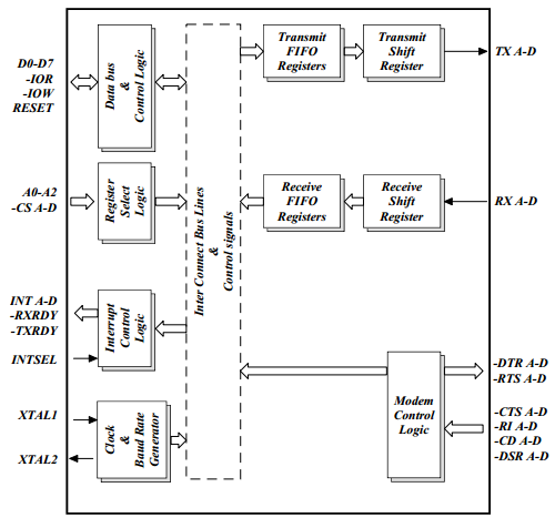
发送数据时,CPU通过通过数据总线写到发送保持寄存器THR中,THR自动组装数据到FIFO,之后每个字节数据通过TSR将并行数据转换为串行bit发送出去。
接收数据时,数据首先到达RSR(接收偏移结存器),RSR组装数据到FIFO中,CPU通过读取RHR接收保持寄存器,把数据一个字节一个字节的读取。
FIFO只能设置触发水平,不能直接访问。TSR/RSR自动完成数据串并转换,CPU不用控制。
寄存器
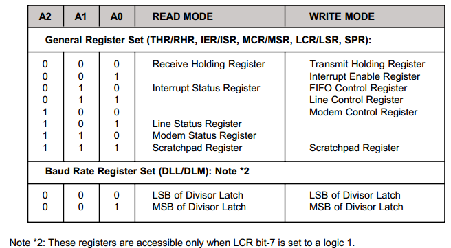
The 554D provides 13 internal registers for monitoring and control.
FIFO
The 16 byte transmit and receive data FIFO’s are enabled by the FIFO Control Register (FCR) bit-0. With 16C554 devices, the user can only set the receive trigger level. The receiver FIFO section includes a time-out function to ensure data is delivered to the external CPU. An interrupt is generated whenever the Receive Holding Register (RHR) has not been read following the loading of a character or the receive trigger level has not been reached.
Interrupts
The interrupts are enabled by IER bits 0-3. Care must be taken when handling these interrupts. Following a reset the transmitter interrupt is enabled, the 554D will issue an interrupt to indicate that transmit holding register is empty. This interrupt must be serviced prior to continuing operations. The LSR register provides the current singular highest priority interrupt only. Servicing the interrupt without investigating further interrupt conditions can result in data errors.
When two interrupt conditions have the same priority, it is important to service these interrupts correctly. Receive Data Ready and Receive Time Out have the same interrupt priority (when enabled by IER bit-0).The receiver issues an interrupt after the number of characters have reached the programmed trigger level. In this case the 554D FIFO may hold more characters than the programmed trigger level. Following the removal of a data byte, the user should recheck LSR bit-0 for additional characters. A Receive Time Out will not occur if the receive FIFO is empty. The time out counter is reset at the center of each stop bit received or each time the receive holding register (RHR) is read.
DMA
LSR bits 5-6 provide an indication when the transmitter is empty or has an empty location(s). The user can optionally operate the transmit and receive FIFOs in the DMA mode (FCR bit-3). When the transmit and receive FIFOs are enabled and the DMA mode is deactivated (DMA Mode “0”), the 554D activates the interrupt output pin for each data transmit or receive operation. When DMA mode is activated (DMA Mode “1”), the user takes the advantage of block mode operation by loading or unloading the FIFO in a block sequence determined by the preset trigger level. In this mode, the 554D sets the interrupt output pin when characters in the transmit FIFOs are below the transmit trigger level, or the characters in the receive FIFOs are above the receive trigger level.
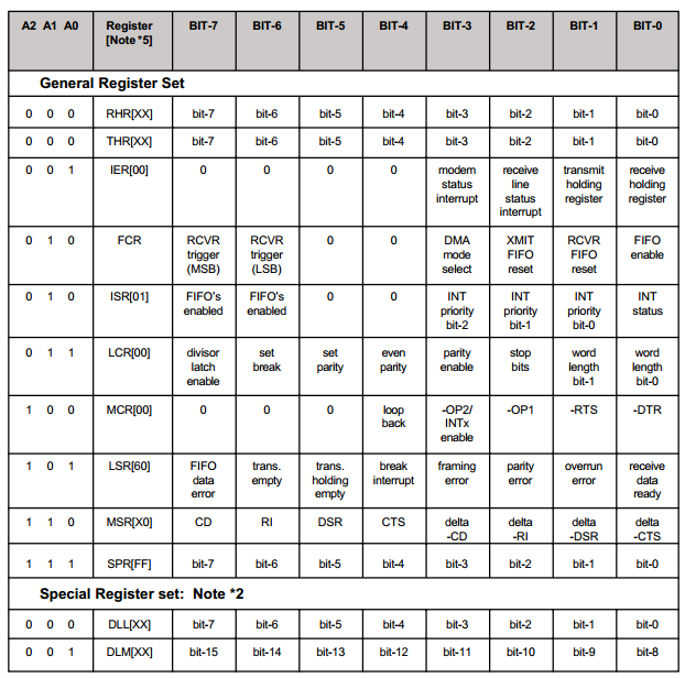
Interrupt Enable Register (IER)
The Interrupt Enable Register (IER) masks the interrupts from receiver ready, transmitter empty, line status and modem status registers. These interrupts would normally be seen on the INT A-D output pins in the 16 mode, or on WIRE-OR IRQ output pin, in the 68 mode.
IER BIT-0: This interrupt will be issued when the FIFO has reached the programmed trigger level or is cleared when the FIFO drops below the trigger level in the FIFO mode of operation.
Logic 0 = Disable the receiver ready interrupt. (normal default condition)
Logic 1 = Enable the receiver ready interrupt.
Interrupt Status Register (ISR)
The 554D provides four levels of prioritized interrupts to minimize external software interaction. The Interrupt Status Register (ISR) provides the user with six interrupt status bits. Performing a read cycle on the ISR will provide the user with the highest pending interrupt level to be serviced. No other interrupts are acknowledged until the pending interrupt is serviced. Whenever the interrupt status register is read, the interrupt status is cleared. However it should be noted that only the current pending interrupt is cleared by the read. A lower level interrupt may be seen after rereading the interrupt status bits. The Interrupt Source Table 7 (below) shows the data values (bit 0-5) for the four prioritized interrupt levels and the interrupt sources associated with each of these interrupt levels:

LSR中断优先级最高,MSR中断优先级最低。
用户可通过读取ISR得知被服务的最高优先级中断,这时,不会响应其他中断,直到该中断被处理完。无论何时读中断状态寄存器,中断状态都会被清除。重新读取中断状态位后才知道待处理的下一个优先级更低的中断源。
复位后,发送器中断被使能,16C554将产生一个中断来表示发送保持寄存器为空,这个中断被处理完后才能继续其他操作。LSR寄存器只能提供一个当前优先级最高的中断。CTS和RTS中断的优先级最低,允许出现高优先级中断将低优先级中断屏蔽的情况,只有在服务完高优先级的中断后,低优先级的中断才能在状态寄存器中反应出来,未深入检测中断条件就服务中断可能造成数据出错。
当2个中断的优先级相同时,必须正确处理这些中断,接收数据就绪中断和接收超时中断的优先级相同,当接收的字符数达到编程设定的触发点时接收器产生一个中断,这样,FIFO可能保存比触发点更多的字符。数据字节移走后,用户应该为另外的字符重新检查LSR[0],如果接收FIFO为空,接收超时就不发生。
ISR BIT-0:
Logic 0 = An interrupt is pending and the ISR contents may be used as a pointer to the appropriate interrupt service routine.
Logic 1 = No interrupt pending. (normal default condition)
ISR BIT 1-3: (logic 0 or cleared is the default condition)
These bits indicate the source for a pending interrupt at interrupt priority levels 1, 2, and 3 (See Interrupt Source Table).
ISR BIT 4-5:
Not used - Initialized to a logic 0.
ISR BIT 6-7: (logic 0 or cleared is the default condition)
These bits are set to a logic 0 when the FIFO is not being used. They are set to a logic 1 when the FIFOs are enabled.
Transmit (THR) and Receive (RHR) Holding Registers
The serial transmitter section consists of an 8-bit Transmit Hold Register (THR) and Transmit Shift Register (TSR). The status of the THR is provided in the Line Status Register (LSR). Writing to the THR transfers the contents of the data bus (D7-D0) to the THR, providing that the THR or TSR is empty. The THR empty flag in the LSR register will be set to a logic 1 when the transmitter is empty or when data is transferred to the TSR. Note that a write operation can be performed when the transmit holding register empty flag is set (logic 0 = FIFO full, logic 1= at least one FIFO location available).
The serial receive section also contains an 8-bit Receive Holding Register, RHR. Receive data is removed from the 554D and receive FIFO by reading the RHR register. Receiver status codes will be posted in the LSR.
IER Vs Receive FIFO Interrupt Mode Operation
When the receive FIFO (FCR BIT-0 = a logic 1) and receive interrupts (IER BIT-0 = logic 1) are enabled, the receive interrupts and register status will reflect the following:
A) The receive data available interrupts are issued to the external CPU when the FIFO has reached the programmed trigger level. It will be cleared when the FIFO drops below the programmed trigger level.
B) FIFO status will also be reflected in the user accessible ISR register when the FIFO trigger level is reached. Both the ISR register status bit and the interrupt will be cleared when the FIFO drops below the trigger level.
C) The data ready bit (LSR BIT-0) is set as soon as a character is transferred from the shift register to the receive FIFO. It is reset when the FIFO is empty.
Line Status Register (LSR)
This register provides the status of data transfers between. the 554D and the CPU.
LSR BIT-0:
Logic 0 = No data in receive holding register or FIFO. (normal default condition)
Logic 1 = Data has been received and is saved in the receive holding register or FIFO.
LSR BIT-1:
Logic 0 = No overrun error. (normal default condition)
Logic 1 = Overrun error. A data overrun error occurred in the receive shift register. This happens when additional data arrives while the FIFO is full.
In this case the previous data in the shift register is overwritten. Note that under this condition the data byte in the receive shift register is not transfered into the FIFO, therefore the data in the FIFO is not corrupted by the error.
LSR BIT-2:
Logic 0 = No parity error. (normal default condition)
Logic 1 = Parity error. The receive character does not have correct parity information and is suspect. In the FIFO mode, this error is associated with the character at the top of the FIFO.
LSR BIT-3:
Logic 0 = No framing error. (normal default condition)
Logic 1 = Framing error. The receive character did not have a valid stop bit(s). In the FIFO mode this error is associated with the character at the top of the FIFO.
LSR BIT-4:
Logic 0 = No break condition. (normal default condition)
Logic 1 = The receiver received a break signal (RX was a logic 0 for one character frame time). In the FIFO mode, only one break character is loaded into the FIFO.
LSR BIT-5:
This bit is the Transmit Holding Register Empty indicator. This bit indicates that the UART is ready to accept a new character for transmission. In addition, this bit causes the UART to issue an interrupt to CPU when the THR interrupt enable is set. The THR bit is set to a logic 1 when a character is transferred from the transmit holding register into the transmitter shift register. The bit is reset to logic 0 concurrently with the loading of the transmitter holding register by the CPU. In the FIFO mode this bit is set when the transmit FIFO is empty; it is cleared when at least 1 byte is written to the transmit FIFO.
LSR BIT-6:
This bit is the Transmit Empty indicator. This bit is set to a logic 1 whenever the transmit holding register and the transmit shift register are both empty. It is reset to logic 0 whenever either the THR or TSR contains adata character. In the FIFO mode this bit is set to onewhenever the transmit FIFO and transmit shift register
are both empty.
LSR BIT-7:
Logic 0 = No Error. (normal default condition)
Logic 1 = At least one parity error, framing error or break indication is in the current FIFO data. This bit is cleared when LSR register is read.
FIFO Control Register (FCR)
This register is used to enable the FIFOs, clear the FIFOs, set the transmit/receive FIFO trigger levels, and select the DMA mode.
The DMA, and FIFO modes are defined as follows:
Mode 0 Set and enable the interrupt for each single transmit or receive operation, and is similar to the ST16C454 mode. Transmit Ready (-TXRDY) will go to a logic 0 when ever an empty transmit space is available in the Transmit Holding Register (THR).
Receive Ready (-RXRDY) will go to a logic 0 whenever the Receive Holding Register (RHR) is loaded with a character.
Mode 1 Set and enable the interrupt in a block mode operation. The transmit interrupt is set when the transmit FIFO is below the programmed trigger level. -TXRDY remains a logic 0 as long as one empty FIFO
location is available. The receive interrupt is set when the receive FIFO fills to the programmed trigger level.
However the FIFO continues to fill regardless of the programmed level until the FIFO is full. -RXRDY remains a logic 0 as long as the FIFO fill level is above the programmed trigger level.
Transmit operation in mode “0”:
When the 554D is in the ST16C450 mode (FIFOs disabled, FCR bit-0 = logic 0) or in the FIFO mode (FIFOs enabled, FCR bit-0 = logic 1, FCR bit-3 = logic 0) and when there are no characters in the transmit FIFO or transmit holding register, the -TXRDY pin will be a logic 0. Once active the -TXRDY pin will go to a logic 1 after the first character is loaded into the transmit holding register.
Receive operation in mode “0”:
When the 554D is in mode “0” (FCR bit-0 = logic 0) or in the FIFO mode (FCR bit-0 = logic 1, FCR bit-3 = logic 0) and there is at least one character in the receive FIFO, the -RXRDY pin will be a logic 0. Once active the -RXRDY pin will go to a logic 1 when there are no more characters in the receiver.
Transmit operation in mode “1”:
When the 554D is in FIFO mode ( FCR bit-0 = logic 1, FCR bit-3 = logic 1 ), the -TXRDY pin will be a logic 1 when the transmit FIFO is completely full. It will be a logic 0 if one or more FIFO locations are empty.
Receive operation in mode “1”:
When the 554D is in FIFO mode (FCR bit-0 = logic 1, FCR bit-3 = logic 1) and the trigger level has been reached, or a Receive Time Out has occurred, the -RXRDY pin will go to a logic 0. Once activated, it will go to a logic 1 after there are no more characters in the FIFO.
FCR BIT-0:
Logic 0 = Disable the transmit and receive FIFO. (normal default condition)
Logic 1 = Enable the transmit and receive FIFO. This bit must be a “1” when other FCR bits are written to or they will not be programmed.
FCR BIT-1:
Logic 0 = No FIFO receive reset. (normal default condition)
Logic 1 = Clears the contents of the receive FIFO and resets the FIFO counter logic (the receive shift register is not cleared or altered). This bit will return to a logic 0 after clearing the FIFO.
FCR BIT-2:
Logic 0 = No FIFO transmit reset. (normal default condition)
Logic 1 = Clears the contents of the transmit FIFO and resets the FIFO counter logic (the transmit shift register is not cleared or altered). This bit will return to a logic 0 after clearing the FIFO.
FCR BIT-3:
Logic 0 = Set DMA mode “0”. (normal default condition)
Logic 1 = Set DMA mode “1”
FCR BIT 4-5:
Not used - Initialized to a logic 0.
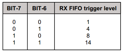
FCR BIT 6-7: (logic 0 or cleared is the default condition, Rx trigger level = 1)
These bits are used to set the trigger level for the receive FIFO interrupt.
An interrupt is generated when the number of characters in the FIFO equals the programmed trigger level. However the FIFO will continue to be loaded until it is full.