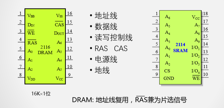
1、SRAM存储单元的不足
晶体管过多
存储密度低
功耗大
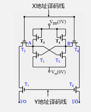
2、DRAM存储单元的基本结构
解决SRAM不足采取的方法:
去掉两个负载管T3、T4
提升存储密度
降低功耗
降低成本
利用栅极分布电容缓冲电荷
增加电路协同存储单元工作
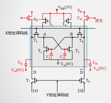
3、DRAM存储单元的工作原理
写操作
Y地址选通
T7、T8管导通
I/O端数据写入到位线
X地址选通
T5、T6管导通
位线与C2、C1相连
读操作:
给出预充信号
T9、T10导通
充电电压给CD充电(充满)
撤除预充信号
X地址选通
T5、T6管导通
右CD通过C1放电
左CD给C2充电
Y地址选通
T7、T8管导通
左CD与右CD间形成放电电流
读过程比写复杂、速度慢
保持操作:
X地址选通信号撤销
Y地址选通信号撤销
栅极电容容量有限,可持续的时间很短。
刷新操作:
给出预充信号
T9、T10导通
充电电压给左右CD充电
撤除预充信号
X地址选通
T5、T6管导通
右CD通过C1放电
左CD给C2充电
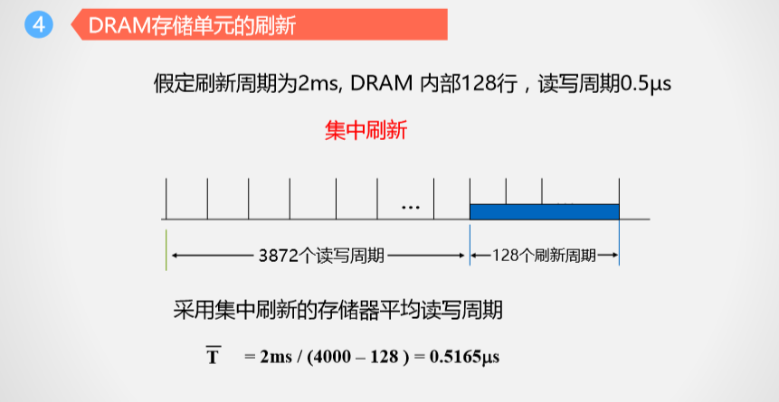
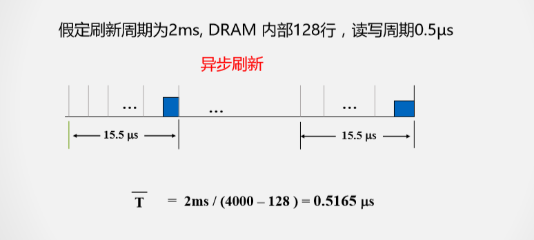
3、DRAM存储单元的刷新
刷新周期:两次刷新之间的时间间隔
双译码结构的DRAM刷新按行进行,需要知道DRAM芯片存储矩阵的行数
刷新地址由刷新地址计数器给出。

5、DRAM与SRAM的对比
6、其他结构的DRAM存储单元
进一步提高存储密度
裁剪冗余电路
核心是电容