csapp 560:
不同层次存储器的区别:
If the data your program needs are stored in a CPU register, then they can be accessed in zero cycles during the execution of the instruction. If stored in a cache, 1 to 30 cycles. If stored in main memory, 50 to 200 cycles. And if stored in disk tens of millions of cycles!
ROM存储的数据是非易失性的。ROM中有的类型既可以读也可以写。
存储在ROM中的程序项目称为固件(firmware)。计算机启动的时候首先读取ROM中的固件内容。
ROM包括闪存卡(flash memory)等
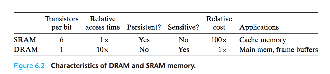
RAM的分类和使用场景:
Random-access memory (RAM) comes in two varieties—static and dynamic. Static RAM (SRAM) is faster and significantly more expensive than Dynamic RAM (DRAM). SRAM is used for cache memories, both on and off the CPU chip. DRAM is used for the main memory plus the frame buffer of a graphics system. Typically, a desktop system will have no more than a few megabytes of SRAM, but hundreds or thousands of megabytes of DRAM.
两者的比较(P562)
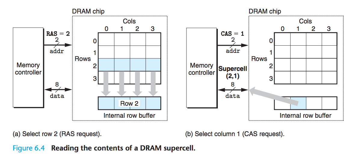
请求DRAM中数据的过程:
假如要请求(2,1)处的数据,那么存储控制器(memory controller,与CPU相连)发送行地址2,DRAM将行为2的整个内容拷贝到一个内部的行缓冲区。接下来,存储控制器发送列地址1,DRAM从行缓冲区中拷贝出(2,1)中的8位,并把他们发送到存储控制器
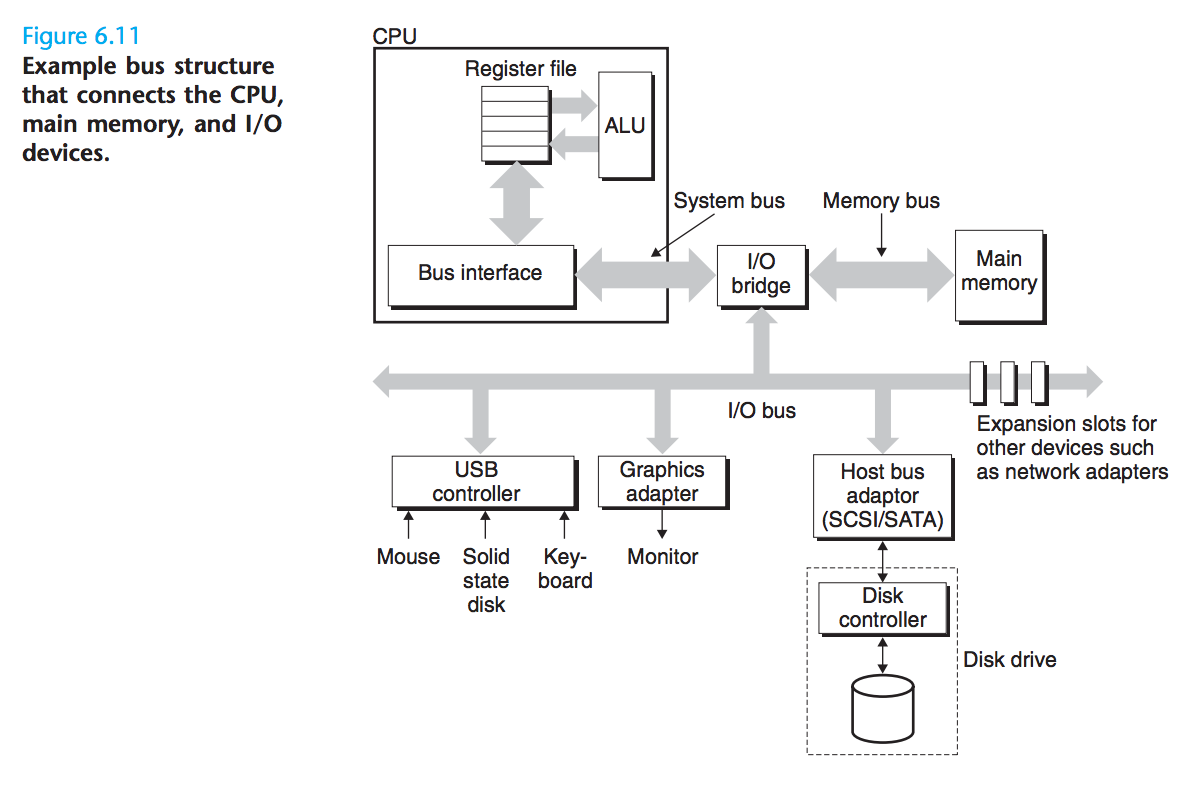
通过总线(bus)访问主存,如下图:
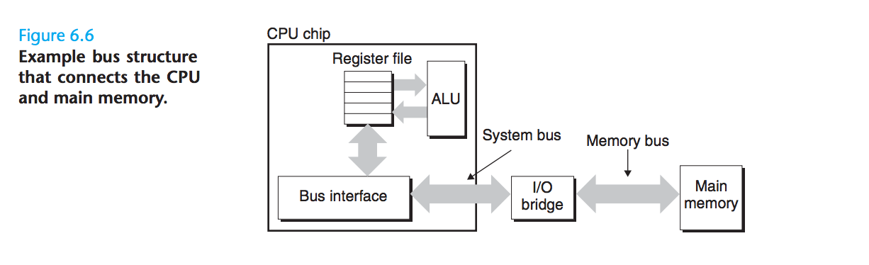
对这个图的解读:
The main components are the CPU chip, a chipset that we will call an I/O bridge (which includes the memory controller), and the DRAM memory modules that make up main memory. These components are connected by a pair of buses: a system bus that connects the CPU to the I/O bridge, and a memory bus that connects the I/O bridge to the main memory.The I/O bridge translates the electrical signals of the system bus into the electrical signals of the memory bus.
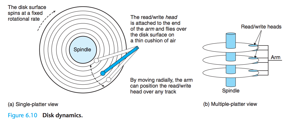
关于硬盘(disk):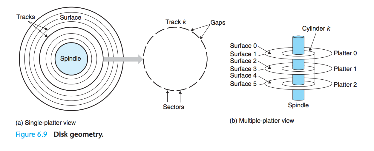
在single-platter(单盘片的情况下):
sector < track < surface < platter
multiple-platter 情况下:
sector < track < cylinder
disk工作过程:
磁盘的access time包括(依次进行):
seek time(找到sector所在的track)
rotational latency(转到sector的第一个位)
transfer time(读取sectors的时间)
其中,前两者时间近似相等,占比最大;transfer time几乎不占用时间
逻辑磁盘块:
读取磁盘的内容是使用磁盘控制器(disk controller)来实现的,这个过程如下:
When the operating system wants to perform an I/O operation such as reading a disk sector into main memory, it sends a command to the disk controller asking it to read a particular logical block number. Firmware on the controller performs a fast table lookup that translates the logical block number into a (surface, track, sector)triple that uniquely identifies the corresponding physical sector. Hardware on the controller interprets this triple to move the heads to the appropriate cylinder, waits for the sector to pass under the head, gathers up the bits sensed by the head into a small memory buffer on the controller, and copies them into main memory.
注意,在OS看来,disk是用logical block number表示的
在磁盘格式化的时候做了什么:
Before a disk can be used to store data, it must be formatted by the disk controller. This involves filling in the gaps between sectors with information that identifies the sectors, identifying any cylinders with surface defects and taking them out of action, and setting aside a set of cylinders in each zone as spares that can be called into action if one or more cylinders in the zone goes bad during the lifetime of the disk. The formatted capacity quoted by disk manufacturers is less than the maximum capacity because of the existence of these spare cylinders.
连接IO设备:
Input/output (I/O) devices are connected to the CPU and main memory using an I/O bus such as Intel’s Peripheral Component Interconnect (PCI) bus.
Although the I/O bus is slower than the system and memory buses, it can accommodate a wide variety of third-party I/O devices.
磁盘也是一种 IO device
CPU如何从disk中读取数据:
首先介绍memorymapped I/O:
The CPU issues commands to I/O devices using a technique called memorymapped I/O (Figure 6.12(a)). In a system with memory-mapped I/O, a block of addresses in the address space is reserved for communicating with I/O devices. Each of these addresses is known as an I/O port. Each device is associated with (or mapped to) one or more ports when it is attached to the bus.
关于CPU从disk中读取数据的过程,CSAPP介绍得非常精彩:
As a simple example, suppose that the disk controller is mapped to port 0xa0. Then the CPU might initiate a disk read by executing three store instructions to address 0xa0: The first of these instructions sends a command word that tells the disk to initiate a read, along with other parameters such as whether to interrupt the CPU when the read is finished. (We will discuss interrupts in Section 8.1.) The second instruction indicates the logical block number that should be read. The third instruction indicates the main memory address where the contents of the disk sector should be stored.
After it issues the request, the CPU will typically do other work while the disk is performing the read. Recall that a 1 GHz processor with a 1 ns clock cycle can potentially execute 16 million instructions in the 16 ms it takes to read the disk. Simply waiting and doing nothing while the transfer is taking place would be enormously wasteful.
After the disk controller receives the read command from the CPU, it translates the logical block number to a sector address, reads the contents of the sector, and transfers the contents directly to main memory, without any intervention from the CPU (Figure 6.12(b)). This process, whereby a device performs a read or write bus transaction on its own, without any involvement (介入)of the CPU, is known as direct memory access (DMA). The transfer of data is known as a DMA transfer.
After the DMA transfer is complete and the contents of the disk sector are safely stored in main memory, the disk controller notifies the CPU by sending an interrupt signal to the CPU (Figure 6.12(c)). The basic idea is that an interrupt signals an external pin on the CPU chip. This causes the CPU to stop what it is currently working on and jump to an operating system routine. The routine records the fact that the I/O has finished and then returns control to the point where the CPU was interrupted.
以及使用SRAM-based caches的原因:
modern computers make heavy use of SRAMbased caches to try to bridge the processor-memory gap.