一、SPI Modes
Serial Peripheral Interface Bus
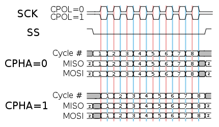
- At CPOL=0 the base value of the clock is zero, i.e. the idle state is 0 and active state is 1.
For CPHA=0, data is captured on the clock's rising edge (low→high transition) and data is changed at the falling edge (high→low transition).
- At CPOL=1 the base value of the clock is one (inversion of CPOL=0), i.e. the idle state is 1 and active state is 0.
For CPHA=1, data is captured on the clock's rising edge (low→high transition) and data is changed at the falling edge (high→low transition).

SPI NAND supports two SPI modes:
• CPOL = 0, CPHA = 0 (Mode 0)
• CPOL = 1, CPHA = 1 (Mode 3)
Input data is latched on the rising edge of SCLK and data shifts out on the falling edge of SCLK for both modes.
Note: While CS# is HIGH, keep SCLK at VCC or GND (determined by mode 0 or mode 3). Do not toggle SCLK until CS# is driven LOW.
在CS#为高(一直保持到active-low)时,SCK即CPOL,决定了colck priority。然后在phase上是一致的,falling发出数据,rising采样。
打算采用全局变量先定义SCK的起始电平,然后1、翻转 SCK<=~SCK 来传输数据;或者 2、先falling出MSB。
二、
//