81.A D flip-flop is a circuit that stores a bit and is updated periodically, at the (usually) positive edge of a clock signal.

D flip-flops are created by the logic synthesizer when a clocked always block is used (See alwaysblock2). A D flip-flop is the simplest form of "blob of combinational logic followed by a flip-flop" where the combinational logic portion is just a wire.
Create a single D flip-flop.
module top_module (
    input clk,    // Clocks are used in sequential circuits
    input d,
    output reg q );//
    always@(posedge clk)
        q<=d;
    // Use a clocked always block
    //   copy d to q at every positive edge of clk
    //   Clocked always blocks should use non-blocking assignments
endmodule
82.Create 8 D flip-flops. All DFFs should be triggered by the positive edge of clk.
module top_module (
    input clk,
    input [7:0] d,
    output [7:0] q
);
    always@(posedge clk)
        q<=d;
endmodule
83.Create 8 D flip-flops with active high synchronous reset. All DFFs should be triggered by the positive edge of clk.
module top_module (
    input clk,
    input reset,            // Synchronous reset
    input [7:0] d,
    output [7:0] q
);
    always@(posedge clk) begin
        if(reset)
            q<=8'b00000000;
        else
            q<=d;
    end
endmodule
84.Create 8 D flip-flops with active high synchronous reset. The flip-flops must be reset to 0x34 rather than zero. All DFFs should be triggered by the negative edge of clk.
Hint:Resetting a register to '1' is sometimes called "preset"
[注]十六进制数的表示方式为0x开头,0x34 = 48+4 = 52=8'b00110100。
module top_module (
    input clk,
    input reset,
    input [7:0] d,
    output [7:0] q
);
    always@(negedge clk) begin
        if(reset)
            q<=8'b00110100;
        else
            q<=d;
    end
endmodule
85.Create 8 D flip-flops with active high asynchronous reset. All DFFs should be triggered by the positive edge of clk.
Hint:The only difference in code between synchronous and asynchronous reset flip-flops is in the sensitivity list.
注意敏感列表写法
module top_module (
    input clk,
    input areset,   // active high asynchronous reset
    input [7:0] d,
    output [7:0] q
);
    always@(posedge areset or posedge clk) begin
        if(areset)
            q<=8'b00000000;
        else
            q<=d;
    end
endmodule
86.Create 16 D flip-flops. It's sometimes useful to only modify parts of a group of flip-flops. The byte-enable inputs control whether each byte of the 16 registers should be written to on that cycle. byteena[1] controls the upper byte d[15:8], while byteena[0] controls the lower byte d[7:0].
resetn is a synchronous, active-low reset.
All DFFs should be triggered by the positive edge of clk.
module top_module (
    input clk,
    input resetn,
    input [1:0] byteena,
    input [15:0] d,
    output [15:0] q
);
    always@(posedge clk) begin
        if (~resetn)
            q<=16'd0;
        else begin
            if (byteena[1])
                q[15:8]<=d[15:8];
            else
                 ;
            if (byteena[0])
                q[7:0]<=d[7:0];
            else
                 ;
        end
    end
endmodule
87.Implement the following circuit:

Note that this is a latch, so a Quartus warning about having inferred a latch is expected.
Hint:
- Latches are level-sensitive (not edge-sensitive) circuits, so in an always block, they use level-sensitive sensitivity lists.
- However, they are still sequential elements, so should use non-blocking assignments.
- A D-latch acts like a wire (or non-inverting buffer) when enabled, and preserves the current value when disabled.
module top_module (
    input d,
    input ena,
    output reg q);

    always@(*) begin
        if (ena)
            q <= d;
    end
endmodule
88.Implement the following circuit:

module top_module (
    input clk,
    input d,
    input ar,   // asynchronous reset
    output q);
    always@(posedge clk or posedge ar) begin
        if (ar)
            q<=0;
        else
            q<=d;
    end
endmodule
89.Implement the following circuit:

module top_module (
    input clk,
    input d,
    input r,   // synchronous reset
    output q);
    always@(posedge clk) begin
        if (r)
            q<=0;
        else
            q<=d;
    end
endmodule
90.Implement the following circuit:

module top_module (
    input clk,
    input in,
    output out);
    wire d;
    always@(posedge clk)
        out<=d;
    assign d=in^out;
endmodule
91.Consider the sequential circuit below:

Assume that you want to implement hierarchical Verilog code for this circuit, using three instantiations of a submodule that has a flip-flop and multiplexer in it. Write a Verilog module (containing one flip-flop and multiplexer) named top_module for this submodule.
module top_module (
    input clk,
    input L,
    input r_in,
    input q_in,
    output reg Q);
    wire d;
    always@(posedge clk)
        Q<=d;
    assign d=(L)?r_in:q_in;
endmodule
92.Consider the n-bit shift register circuit shown below:

Write a Verilog module named top_module for one stage of this circuit, including both the flip-flop and multiplexers.
module top_module (
    input clk,
    input w, R, E, L,
    output Q
);
    wire d1,d2;
    always@(posedge clk)
        Q<=d2;
    assign d1=(E)?w:Q;
    assign d2=(L)?R:d1;
endmodule

//PS.20.07.18
module top_module (
    input clk,
    input w, R, E, L,
    output Q
);
    always@(posedge clk) begin
        case({E,L})
            2'b00:Q<=Q;
            2'b01:Q<=R;
            2'b10:Q<=w;
            2'b11:Q<=R;
        endcase
    end
endmodule
93.Given the finite state machine circuit as shown, assume that the D flip-flops are initially reset to zero before the machine begins.
Build this circuit.

module top_module (
    input clk,
    input x,
    output z
);
    wire d1,d2,d3;
    reg q1=0,q2=0,q3=0;
    assign d1 = q1^x;
    assign d2 = x&~q2;
    assign d3 = x|~q3;
    dff dff1 (d1,clk,q1);
    dff dff2 (d2,clk,q2);
    dff dff3 (d3,clk,q3);
    assign z = ~(q1|q2|q3);
endmodule

module dff (input d,
    input clk,
    output reg q);
    always@(posedge clk) begin
        q <= d;
    end
endmodule
//因为没设定初始值错了好多次;
94.A JK flip-flop has the below truth table. Implement a JK flip-flop with only a D-type flip-flop and gates. Note: Qold is the output of the D flip-flop before the positive clock edge.

module top_module (
    input clk,
    input j,
    input k,
    output Q);
    always@(posedge clk)
        case ({j,k})
            2'b00: ;
            2'b01: Q <= 0;
            2'b10: Q <= 1;
            2'b11: Q <= ~Q;
        endcase
endmodule
95.For each bit in an 8-bit vector, detect when the input signal changes from 0 in one clock cycle to 1 the next (similar to positive edge detection). The output bit should be set the cycle after a 0 to 1 transition occurs.
Here are some examples. For clarity, in[1] and pedge[1] are shown separately.

module top_module ( input clk, input [7:0] in, output [7:0] pedge ); reg [7:0] d; always@(posedge clk) begin d <= in; pedge <= (~d)∈ end endmodule
96.For each bit in an 8-bit vector, detect when the input signal changes from one clock cycle to the next (detect any edge). The output bit should be set the cycle after a 0 to 1 transition occurs.
Here are some examples. For clarity, in[1] and anyedge[1] are shown separately.
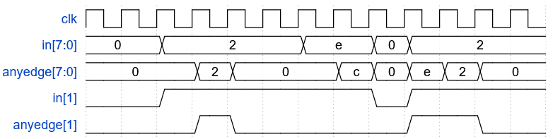
module top_module (
    input clk,
    input [7:0] in,
    output [7:0] anyedge
);
    reg [7:0] d;
    always@(posedge clk) begin
        d <= in;
        anyedge <= d^in;
    end
endmodule