转载:原文 http://www.eefocus.com/antaur/blog/17-08/423751_6cc0d.html
0. 引言
通过之前的学习,可以在PL端创建从机模式的AXI接口IP核。但是从机模式是被动接收数据,而不能主动的去获取数据,因此计划研究一下AXI Master接口的IP核的构建方法。
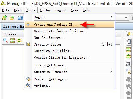
1. 利用向导创建AXI Lite Master测试用例
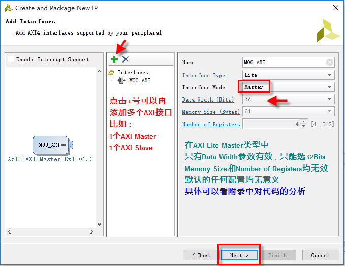
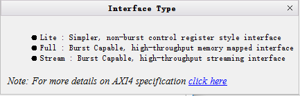
在这一步,AXI类型为Lite型的,可选参数如下所示:
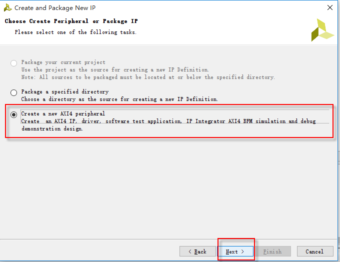
在这里,重点是Interface Mode,前面的实验中采用的是默认配置Slave,即设计的IP接口为从机。本实验中,要将其设置为Master。
下面的三个参数跟Sl**e模式下可配置的参数类型是相同的。具体的说明如下所示:
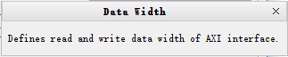
Data Width:为数据总线的位宽,单位为bits
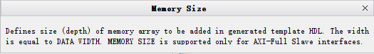
Memory Size:只有在IP类型为AXI FULL Slave模式下才有效,目前不讨论。
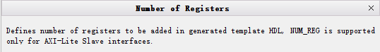
Number of Registers:只有在IP接口类型为AXI Lite Slave模式下才有效,可以参看之前的实验说明。
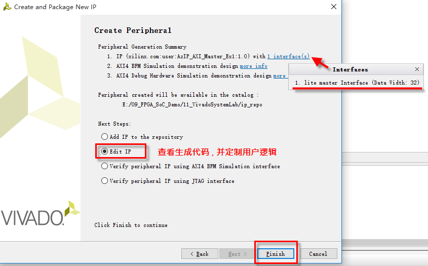
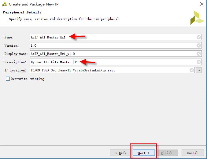
至此,利用向导工具创建一个AXI Lite Master类型的IP接口配置完毕。
2. 源码分析
2.1 顶层源码解析
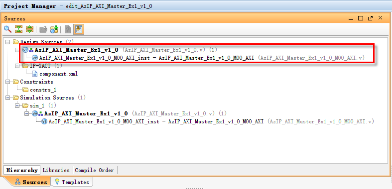
系统会自动生成一个该IP的工程,可以查看生成的源代码,并在此基础上进行修改。
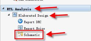
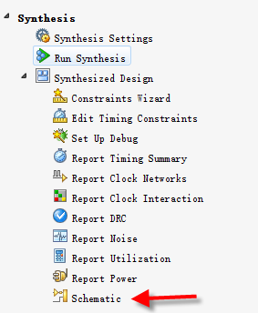
从上图可以看出,向导工具就生成了两个模块。直接综合后,查看RTL级图的操作入口如下所示:
显示结果如下:
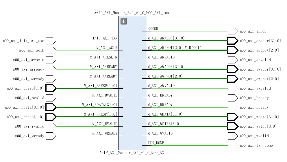
可以看出顶层模块只是做了简单的直连封装,内部没有任何逻辑设计,查看代码(附录1)也是如此,唯一有用的操作配置了内层模块实例的参数。
具体配置测参数如下所示:
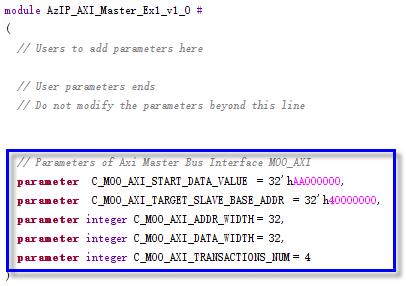
可以看到配置了5个参数,其中:
C_M00_AXI_ADDR_WIDTH表示地址总线的位宽,这里配置为32bits,由于涉及到总线的协议,建议不要动这个参数。
C_M00_AXI_DATA_WIDTH表示数据总线的位宽,这里配置为32bits,同样的原因,建议不要动这个参数。
其余的三个参数是根据测试用例的用户逻辑相关的,具体意义在底层模块的源码分析(附录2)中会详细解释,这里简单说明一下:
C_M00_AXI_TARGET_SLAVE BASE_ADDR表示本IP作为主机欲访问的从机内存的基地址。
C_M00_AXI_START_DATA_VALUE表示对从机寄存器进行写入操作的测试数据
C_M00_AXI_TRANSACTIONS_NUM表示测试的次数
具体逻辑及各参数的意义见下文对底层模块的解析。
2.2 底层源码解析
向导自动生成的示例程序中底层模块为AzIP_AXI_Master_Ex1_v1_0_M00_AXI,该模块并不是一个Master型的IO标准接口,而只是一个用户测试用例的逻辑操作。而Master的Write和Read读写逻辑并没有很完毕的封装,需要仔细分析示例代码进行拆分。
具体的代码解析详见后面附录2的注释说明,这里给出的仅是本人对此分析得到的笔记。
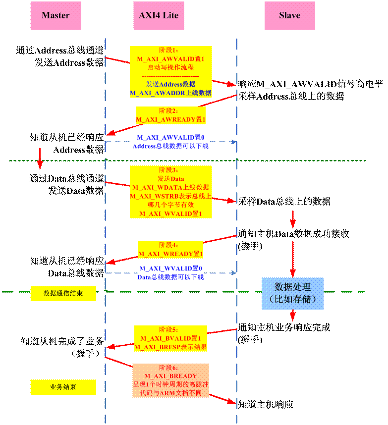
- 测试业务逻辑
测试业务逻辑的本质如下图所示,就是一个典型的内存读写操作的测试流程。
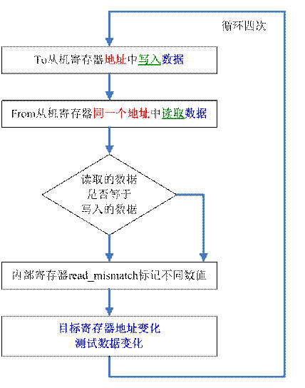
代码编写时采用状态机的方式。
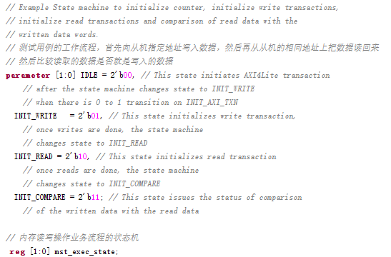
其中:
【地址操作分析】:
从机寄存器的初始地址有变量C_M00_AXI_TARGET_SLAVE_BASE_ADDR定义,在构建集成系统时,对应从机的内存映射必须于配置相同。
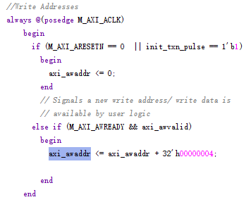
AXI总线上写操作地址总线绑定如下,C_M00_AXI_TARGET_SLAVE_BASE_ADDR为基地址,而axi_awaddr定义地址偏移量。
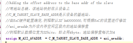

段内地址偏移量初始化值为0,每次写入成功后,地址偏移量+4,这是因为地址定义的单位是字节Byte,而数据总线为32bits,即4个字节,因此没写入32bits,会用掉从机4个地址的存储空间。
关于读取操作指定寄存器的地址定义及处理过程是类似的。
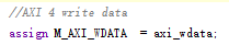
【数据操作分析】:
写操作使用的数据总线绑定到一个内部寄存器上。
初始化时,测试数据寄存器被设置为参数配置的数值,之后每次加1。
测试数据向从机写入之后,内部备份保存一份,存在寄存器expected_rdata中,代码如下:
可以看到代码逻辑完全相同,但是整个代码架构真的不敢苟同。
数据比较段的代码如下:
相应的逻辑应该是一旦有一次出错,read_mismatch就置为1,如果下次对了,该状态寄存器仍然保持数据为1,直到复位操作。
(2)AXI4-Lite总线接口定义
在进行AXI4-Lite总线读写时序操作时,首先要明确总线的读写操作接口。
查看相关技术文档,这里主要用到以下两个技术文档:
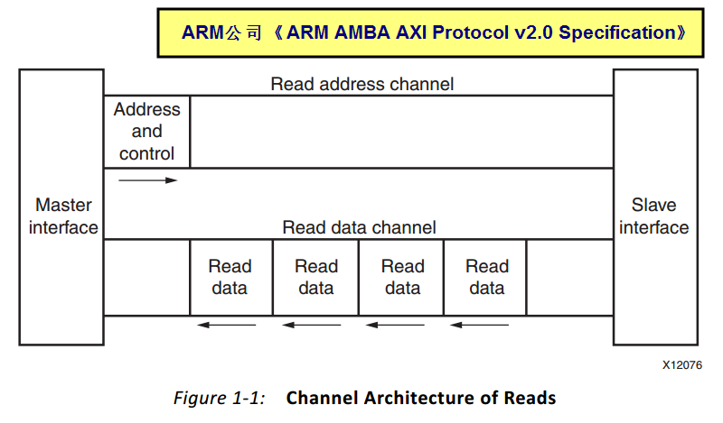
- ARM公司发布的《ARM AMBA AXI Protocol v2.0 Specification》
- Xilinx公司发布的《Vivado Design Suite : AXI Reference Guide》UG1037(v3.0)2015
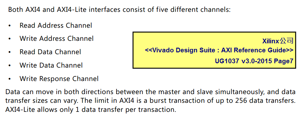
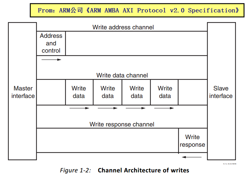
可以看到,无论是AXI4总线还是精简版的AXI4-Lite总线接口分成5大类,这5大类又分别****于Write操作核Read操作。
Write操作
- 写地址:主机-->从机
- 写数据:主机-->从机
- 写应答:从机-->主机
Read操作
- 读地址:主机-->从机
- 读数据:从机-->主机
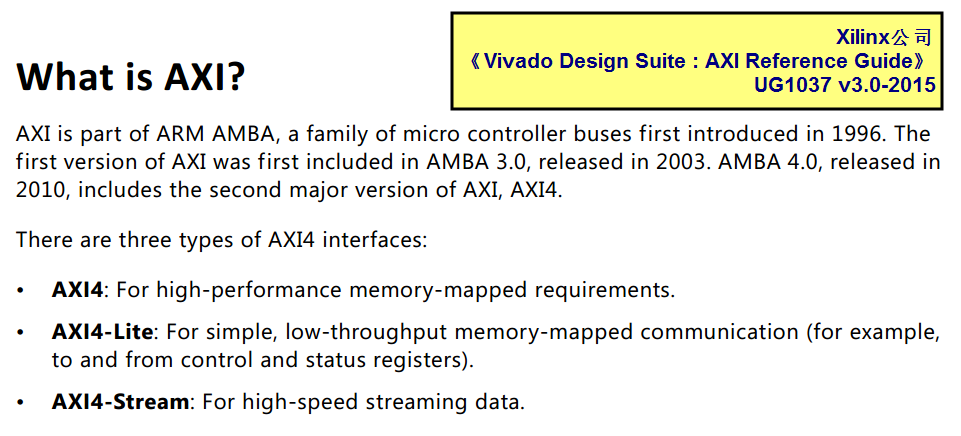
下面重点研究一下AXI4-Lite总线具体是如何定义的,它与AXI4总线协议有什么不同?
首先看一下AXI4总线协议的官方定义:
再看一下AXI4-Lite总线协议的官方定义:
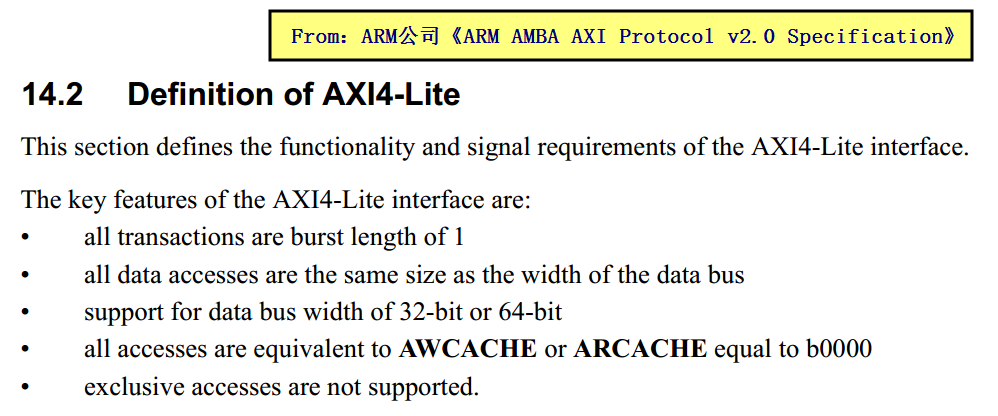
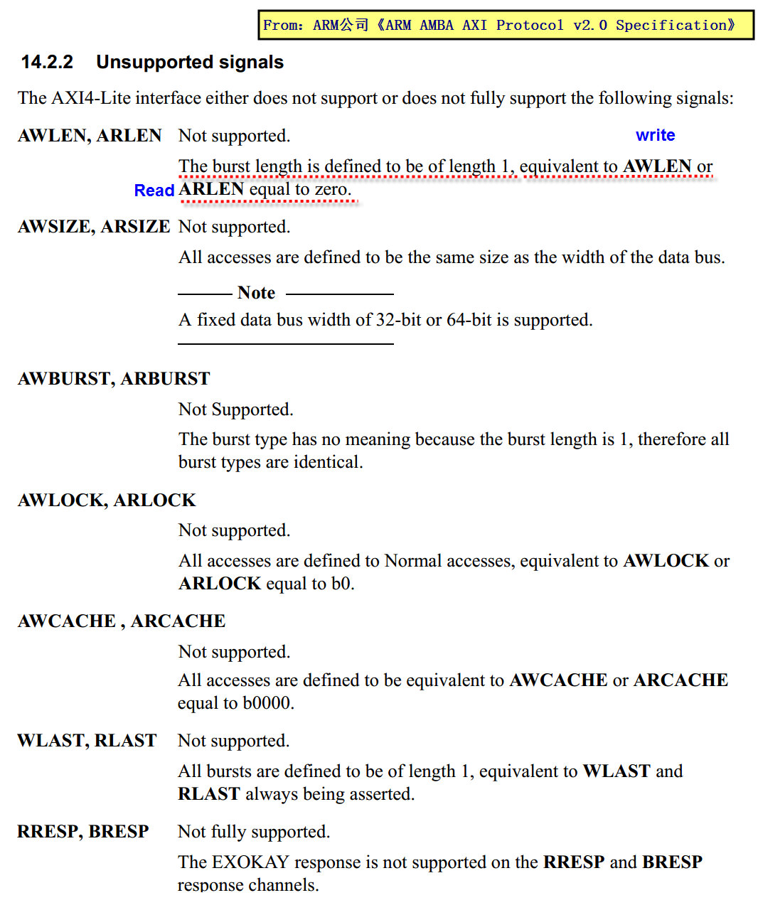
不支持突发(burst)传输模式,及burst length=1
数据总线宽度只能为32bit或则64bits
不支持独家访问(exclusive accesses)
即AXI4-Lite不支持突发(burst)传输模式。
【说明】关于突发(burst)传输模式是否采用将在后面分析读写时序时重点讨论。这里先铺垫一下。
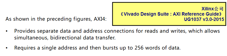
AXI4总线,由于读写通道是分离的,可以提供实时双向的数据传输。
采用突发(burst)传输模式,可以在发送1个地址之后,最多支持突发256words的数据。(Words??2字节吗??)
下面看一下AXI4-Lite总线协议的物理接口Port的定义:
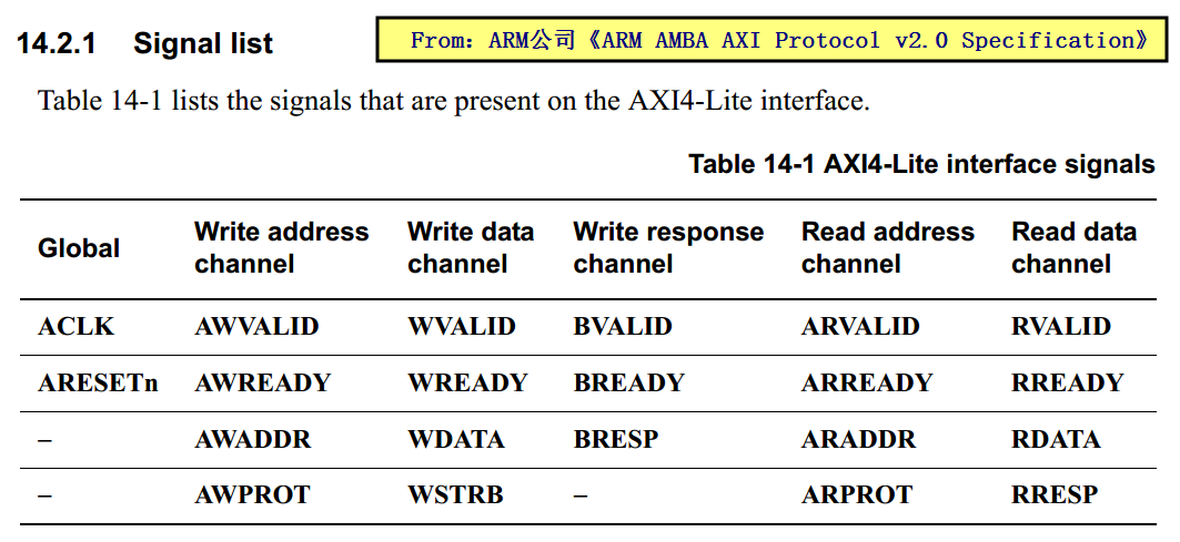
可以看出除了时钟和复位信号后,也是前文介绍的5类信号通道。
但是作为一个简化的总线协议,其物理接口应该比完整版的AXI4总线要少,具体精简掉了哪些?详见下表。
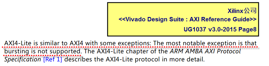
学习完原理性的基础知识之后,我们来看一下示例程序代码是否符合官方标准。
分析AXI Master示例IP源代码的Port定义,代码即注释说明如下所示:
【AXI4-Lite Write Address Channel】
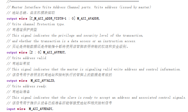
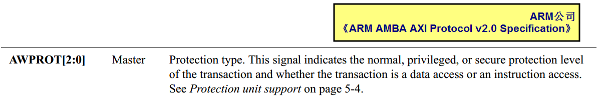
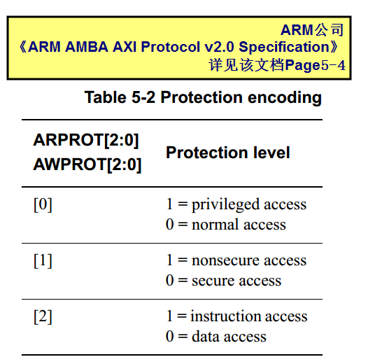
在示例程序中,AXI Master模块的M_AXI_AWPROT管脚始终输出为:3’b000
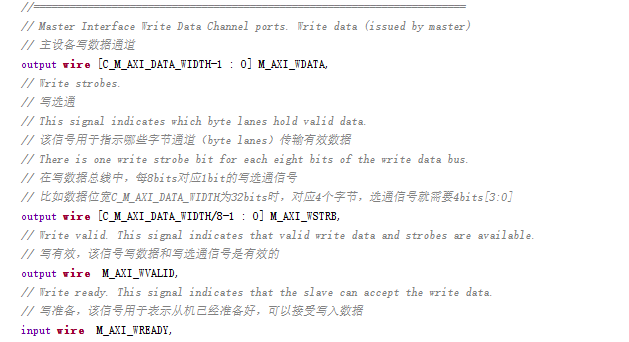
【AXI4-Lite Write data Channel】
其中端口M_AXI_ARPROT,参见【AXI4-Lite Write Address Channel】中的M_AXI_AWPROT
【AXI4-Lite Read Data Channel】
在示例程序中,AXI Master模块由于数据总线位宽为32bit,因此M_AXI_WSTRB管脚始终输出为:4’b1111
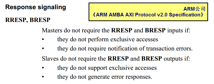
【AXI4-Lite Write response Channel】
【AXI4-Lite Read Address Channel】
其中端口M_AXI_ARPROT,参见【AXI4-Lite Write Address Channel】中的M_AXI_AWPROT
【AXI4-Lite Read Data Channel】
其中端口M_AXI_RRESP,参见【AXI4-Lite Write response Channel】中的M_AXI_BRESP
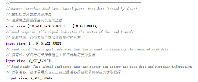
其中端口M_AXI_RRESP,参见【AXI4-Lite Write response Channel】中的M_AXI_BRESP
(3)AXI4-Lite总线读写时序分析1--写入操作时序
研究总线协议的交互时序,必须依赖协议标准,但是能够查到的官方协议标准均没有对AXI4-Lite总线的读写时序进行独立的时序设定。
Xilinx公司发布的文档,引用的还是ARM公司发布的文档,对于总线写入时序逻辑示意图如下:
表示,主机需要先写地址,然后写入一系列数据,为什么是四个暂时不确定,从机处理完毕后回复一个应答响应。
ARM公司发布的文档《ARM AMBA AXI Protocol v2.0 Specification》中没有AXI4-Lits的写入时序逻辑,只有Write brust的时序示意图。如下所示
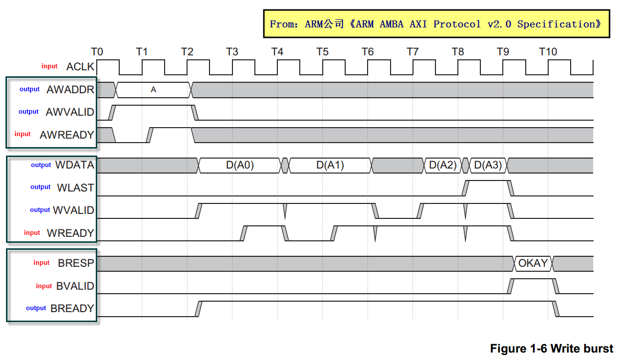
经过前面的研究,知道AXI4-Lite是brust length=1的Write brust,因此我自行简化上述时序图如下:
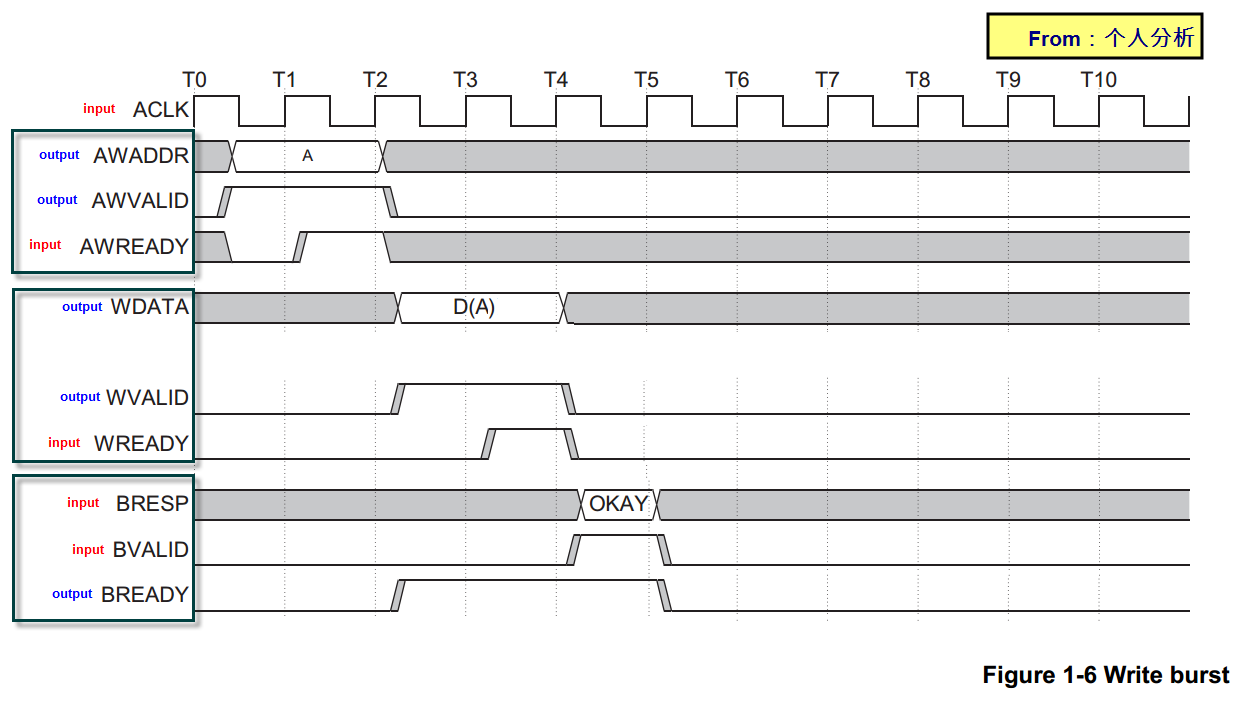
如果主机连续发送两次数据写入操作,我猜测的时序逻辑图应该如下所示:
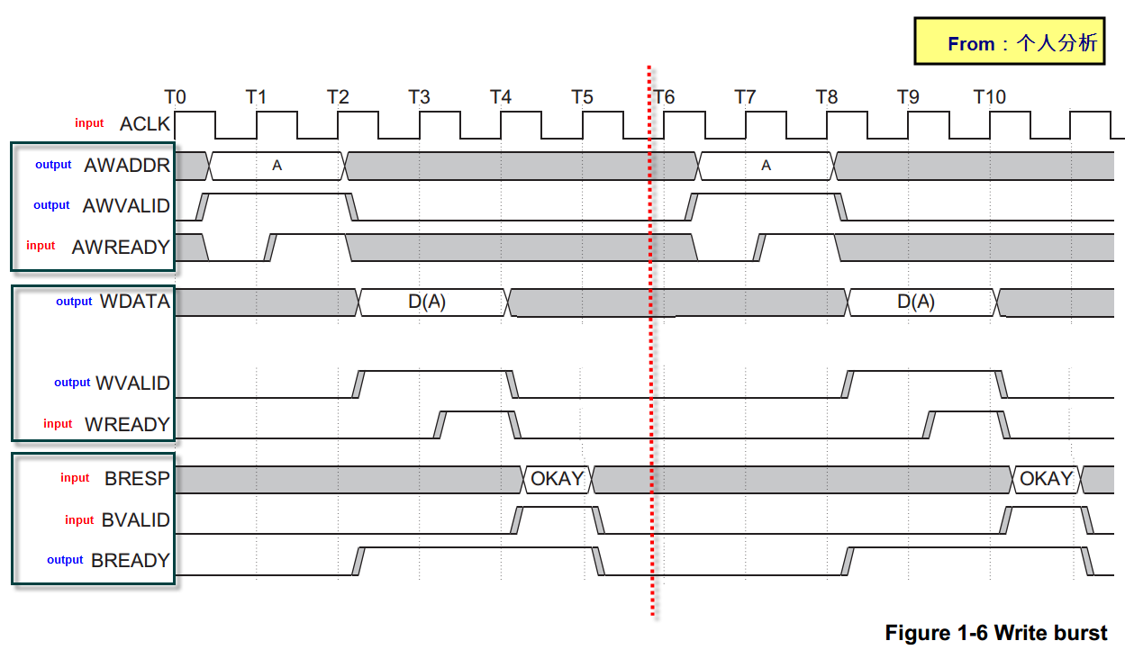
分析示例程序中,AXI Master模块的源代码,绘制相应的主机向从机写入数据的时序逻辑如下图所示:
查看代码,分析得到的时序与个人分析得到的原理时序并不完全匹配。这里先铺垫一下,后文将会对示例源码的时序进行仿真分析,得到对应可用的时序,用于将来自行编写接口时使用。记得看下文。
(4) AXI4-Lite总线读写时序分析2--读取操作时序
同样先学习一下官方协议。
以及来自官方文档的读取操作时序图。

同样自行分析对于brust length=1的AXI4-Lite总线,读取操作的时序图如下所示
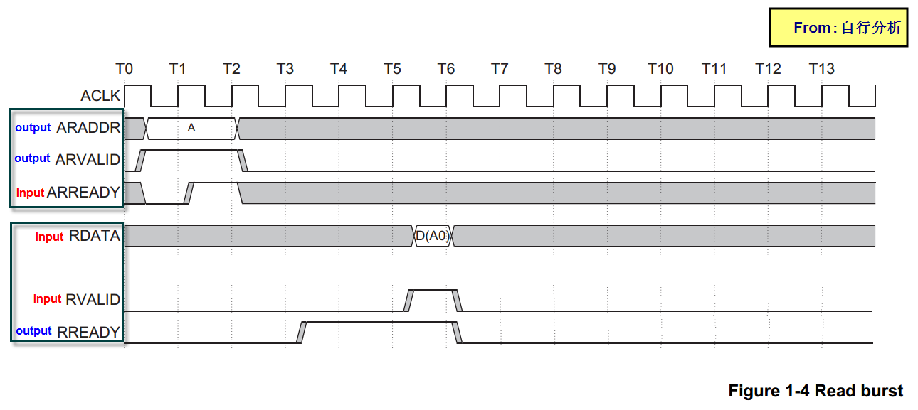
示例代码的操作时序这里就不在画处理流程图了。下文会通过时序仿真给出示例中采用的时序关系。
(5) 示例工程的时序分析
【工程创建的原始出发点】:
根据上述对AXI4-Lite总线接口的分析,其实就是主机和从机之间的数据通信。联想到之间创建的AXI4-Lite Sl**e示例IP核,是否能创建一个顶层模块直接将AXI4-Lite Sl**e示例IP核与AXI4-Lite Sl**e示例IP核直接相连,完成AXI4-Lite总线读写操作?
为了验证上述想法,首先再创建一个AXI4-Lite Sl**e示例IP核,参数要与AXI4-Lite Master示例IP核的参数向对应,下面将端口定义对比如下:
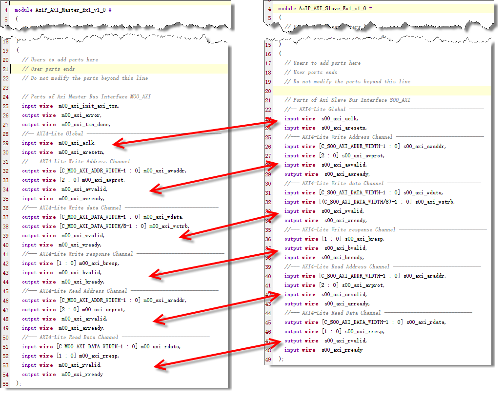
从上图的对比中,可以看出AXI4-Lite主从机的接口其实是一一匹配的。
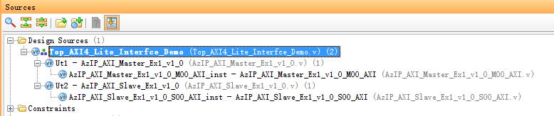
创建一个顶层文件Top_AXI4_Lite_Interfce_Demo,将生成的主从示例直接对连。代码见附录3.相应的层级结构如下图所示。
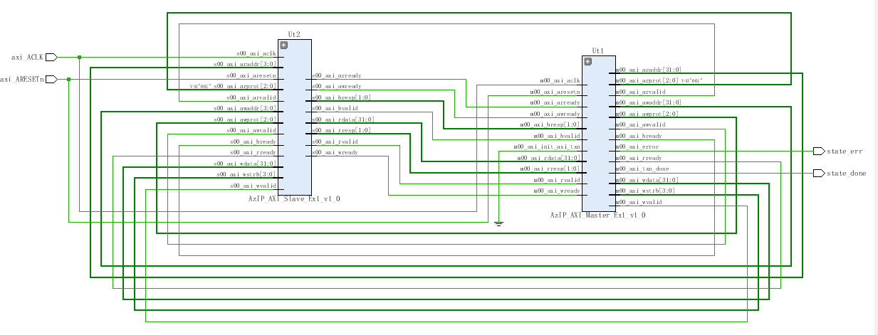
综合完的RTL级连接图如下所示。
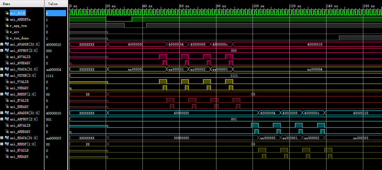
对该顶层文件创建仿真驱动,代码如下所示:
`timescale 1ns / 1ps

module Sim_AXI4_Lite_Interface();
  reg axi_ACLK;    // AXI总线时钟
  reg axi_ARESETn;   // 系统复位信号,低电平有效
  reg r_app_txn;    // 应用级复位信号,负脉冲,上升沿复位
  wire w_err;       // 状态指示,异常
  wire w_txn_done;  // 状态指示,发送完毕
  Top_AXI4_Lite_Interfce_Demo Ut1 (

      .axi_ACLK(axi_ACLK),
      .axi_ARESETn(axi_ARESETn),
      .app_TXn(r_app_txn),
      .state_err(w_err),
      .state_done(w_txn_done)
      );

  parameter PERIOD = 2;

  always begin
    #(PERIOD/2);
    axi_ACLK = ~axi_ACLK;
  end

  initial begin
    axi_ACLK    = 1'b0;
    axi_ARESETn = 1'b1;
    r_app_txn   = 1'b1;
    #(10*PERIOD);
    axi_ARESETn = 1'b0;
    #(5*PERIOD);
    r_app_txn = 1'b0;
    #(2*PERIOD);
    axi_ARESETn = 1'b1;
    #(4*PERIOD);
    r_app_txn = 1'b1;
  end
endmodule
运行后的仿真结果如下所示:
仿真结果1:先写入4次,然后读取4次的时序仿真结果
仿真结果2:先写入1次,然后读取1次的时序仿真结果
仿真结果3:仅写入1次时序仿真结果
仿真结果4:仅读取1次时序仿真结果
仿真结果5:先写入2次,再读取2次时序仿真结果
- 对比仿真得到的写入操作时序和从官网文档分析得到的时序
【个人心得】
可以看出,AXI4中设定的5类通道都是相互独立的,示例仿真中,应为AWVALID和WVALID是同时给从机的,从机就同时采样AWADDR总线和WDATA总线数据,并同时给出了应答AWREADY和WREADY。
从机在匹配完Address和Data后,给出应答BVALID。
而官方文档上的时序时先发地址后发数据,正常的从机也是能够正确响应的。
结论,自行编写接口时,每个通道要独立处理,不要耦合到一起。
- 对比仿真得到的读取操作时序和从官网文档分析得到的时序
【个人心得】
由于没有经过总线控制器,而是直连的,因此时序仿真结果图中从机的响应速度很快,而原理图中有个响应处理延时。
2. 总结
通过本学习笔记,详细分析了AXI4-Lite总线主机端的交互处理时序,以后就可以自行编写主从机的接口了。
附录1:顶层模块源代码:
`timescale 1ns / 1ps module Top_AXI4_Lite_Interfce_Demo #( parameter C_AXI_START_DATA_VALUE = 32'hAA000000, parameter C_AXI_TARGET_SLAVE_BASE_ADDR = 32'h40000000, parameter integer C_AXI_ADDR_WIDTH = 32, parameter integer C_AXI_DATA_WIDTH = 32, parameter integer C_AXI_TRANSACTIONS_NUM = 4 ) ( input axi_ACLK, input axi_ARESETn, input app_TXn, output state_err, output state_done ); wire w_err; // 状态指示,异常 wire w_txn_done; // 状态指示,发送完毕 assign state_err = w_err; assign state_done = w_txn_done;
wire [C_AXI_ADDR_WIDTH-1 : 0] axi_AWADDR; // AXI总线信号:AWADDR wire [2 : 0] axi_AWPROT; // AXI总线信号:AWPROT wire axi_AWVALID; // AXI总线信号:AWVALID wire axi_AWREADY; // AXI总线信号:AWREAD wire [C_AXI_DATA_WIDTH-1 : 0] axi_WDATA; // AXI总线信号:WDATA wire [C_AXI_DATA_WIDTH/8-1 : 0] axi_WSTRB; // AXI总线信号:WSTRB wire axi_WVALID; // AXI总线信号:WVALID wire axi_WREADY; // AXI总线信号:WREADY wire [1 : 0] axi_BRESP; // AXI总线信号:BRESP wire axi_BVALID; // AXI总线信号:BVALID wire axi_BREADY; // AXI总线信号:BREADY wire [C_AXI_ADDR_WIDTH-1 : 0] axi_ARADDR; // AXI总线信号:ARADDR wire [2 : 0] axi_ARPROT; // AXI总线信号:ARPROT wire axi_ARVALID; // AXI总线信号:ARVALID wire axi_ARREADY; // AXI总线信号:ARREADY wire [C_AXI_DATA_WIDTH-1 : 0] axi_RDATA; // AXI总线信号:RDATA wire [1 : 0] axi_RRESP; // AXI总线信号:RRESP wire axi_RVAILD; // AXI总线信号:RVAILD wire axi_RREADY; // AXI总线信号:RREADY
axi_ip_master_v1_0 # ( .C_M00_AXI_START_DATA_VALUE(C_AXI_START_DATA_VALUE), .C_M00_AXI_TARGET_SLAVE_BASE_ADDR(C_AXI_TARGET_SLAVE_BASE_ADDR), .C_M00_AXI_ADDR_WIDTH(C_AXI_ADDR_WIDTH), .C_M00_AXI_DATA_WIDTH(C_AXI_DATA_WIDTH), .C_M00_AXI_TRANSACTIONS_NUM(C_AXI_TRANSACTIONS_NUM) ) Ut1 ( //-- AXI4-Lite Global ---------------------------------------------- .m00_axi_aclk(axi_ACLK), .m00_axi_aresetn(axi_ARESETn), //------------------------------------------------------------------ .m00_axi_init_axi_txn(app_TXn), .m00_axi_error(w_err), .m00_axi_txn_done(w_txn_done), //--- AXI4-Lite Write Address Channel ------------------------------ .m00_axi_awaddr(axi_AWADDR), .m00_axi_awprot(axi_AWPROT), .m00_axi_awvalid(axi_AWVALID), .m00_axi_awready(axi_AWREADY), //--- AXI4-Lite Write data Channel ------------------------------ .m00_axi_wdata(axi_WDATA), .m00_axi_wstrb(axi_WSTRB), .m00_axi_wvalid(axi_WVALID), .m00_axi_wready(axi_WREADY), //--- AXI4-Lite Write response Channel ------------------------------ .m00_axi_bresp(axi_BRESP), .m00_axi_bvalid(axi_BVALID), .m00_axi_bready(axi_BREADY), //--- AXI4-Lite Read Address Channel ------------------------------ .m00_axi_araddr(axi_ARADDR), .m00_axi_arprot(axi_ARPROT), .m00_axi_arvalid(axi_ARVALID), .m00_axi_arready(axi_ARREADY), //--- AXI4-Lite Read Data Channel ------------------------------ .m00_axi_rdata(axi_RDATA), .m00_axi_rresp(axi_RRESP), .m00_axi_rvalid(axi_RVAILD), .m00_axi_rready(axi_RREADY) ); axi_ip_slave_v1_0 # ( .C_S00_AXI_DATA_WIDTH(C_AXI_ADDR_WIDTH), .C_S00_AXI_ADDR_WIDTH(7) ) Ut2 ( //-- AXI4-Lite Global ---------------------------------------------- .s00_axi_aclk(axi_ACLK), .s00_axi_aresetn(axi_ARESETn), //--- AXI4-Lite Write Address Channel ------------------------------ .s00_axi_awaddr(axi_AWADDR[6:0]), //注意:只有段地址!!!!!,做的axi_slave_ip的地址位宽为7,寄存器个数为32 .s00_axi_awprot(axi_AWPROT), .s00_axi_awvalid(axi_AWVALID), .s00_axi_awready(axi_AWREADY), //--- AXI4-Lite Write data Channel -------------------------------- .s00_axi_wdata(axi_WDATA), .s00_axi_wstrb(axi_WSTRB), .s00_axi_wvalid(axi_WVALID), .s00_axi_wready(axi_WREADY), //--- AXI4-Lite Write response Channel ------------------------------ .s00_axi_bresp(axi_BRESP), .s00_axi_bvalid(axi_BVALID), .s00_axi_bready(axi_BREADY), //--- AXI4-Lite Read Address Channel ------------------------------ .s00_axi_araddr(axi_ARADDR), .s00_axi_arprot(axi_ARPROT), .s00_axi_arvalid(axi_ARVALID), .s00_axi_arready(axi_ARREADY), //--- AXI4-Lite Read Data Channel ------------------------------ .s00_axi_rdata(axi_RDATA), .s00_axi_rresp(axi_RRESP), .s00_axi_rvalid(axi_RVAILD), .s00_axi_rready(axi_RREADY) ); endmodule 附录2:底层模块MASTER 顶层源代码: `timescale 1 ns / 1 ps module axi_ip_master_v1_0 # ( // Users to add parameters here // User parameters ends // Do not modify the parameters beyond this line // Parameters of Axi Master Bus Interface M00_AXI parameter C_M00_AXI_START_DATA_VALUE = 32'hAA000000, parameter C_M00_AXI_TARGET_SLAVE_BASE_ADDR = 32'h40000000, parameter integer C_M00_AXI_ADDR_WIDTH = 32, parameter integer C_M00_AXI_DATA_WIDTH = 32, parameter integer C_M00_AXI_TRANSACTIONS_NUM = 4 ) ( // Users to add ports here // User ports ends // Do not modify the ports beyond this line // Ports of Axi Master Bus Interface M00_AXI input wire m00_axi_init_axi_txn, output wire m00_axi_error, output wire m00_axi_txn_done, input wire m00_axi_aclk, input wire m00_axi_aresetn, output wire [C_M00_AXI_ADDR_WIDTH-1 : 0] m00_axi_awaddr, output wire [2 : 0] m00_axi_awprot, output wire m00_axi_awvalid, input wire m00_axi_awready, output wire [C_M00_AXI_DATA_WIDTH-1 : 0] m00_axi_wdata, output wire [C_M00_AXI_DATA_WIDTH/8-1 : 0] m00_axi_wstrb, output wire m00_axi_wvalid, input wire m00_axi_wready, input wire [1 : 0] m00_axi_bresp, input wire m00_axi_bvalid, output wire m00_axi_bready, output wire [C_M00_AXI_ADDR_WIDTH-1 : 0] m00_axi_araddr, output wire [2 : 0] m00_axi_arprot, output wire m00_axi_arvalid, input wire m00_axi_arready, input wire [C_M00_AXI_DATA_WIDTH-1 : 0] m00_axi_rdata, input wire [1 : 0] m00_axi_rresp, input wire m00_axi_rvalid, output wire m00_axi_rready ); // Instantiation of Axi Bus Interface M00_AXI axi_ip_master_v1_0_M00_AXI # ( .C_M_START_DATA_VALUE(C_M00_AXI_START_DATA_VALUE), .C_M_TARGET_SLAVE_BASE_ADDR(C_M00_AXI_TARGET_SLAVE_BASE_ADDR), .C_M_AXI_ADDR_WIDTH(C_M00_AXI_ADDR_WIDTH), .C_M_AXI_DATA_WIDTH(C_M00_AXI_DATA_WIDTH), .C_M_TRANSACTIONS_NUM(C_M00_AXI_TRANSACTIONS_NUM) ) axi_ip_master_v1_0_M00_AXI_inst ( .INIT_AXI_TXN(m00_axi_init_axi_txn), .ERROR(m00_axi_error), .TXN_DONE(m00_axi_txn_done), .M_AXI_ACLK(m00_axi_aclk), .M_AXI_ARESETN(m00_axi_aresetn), .M_AXI_AWADDR(m00_axi_awaddr), .M_AXI_AWPROT(m00_axi_awprot), .M_AXI_AWVALID(m00_axi_awvalid), .M_AXI_AWREADY(m00_axi_awready), .M_AXI_WDATA(m00_axi_wdata), .M_AXI_WSTRB(m00_axi_wstrb), .M_AXI_WVALID(m00_axi_wvalid), .M_AXI_WREADY(m00_axi_wready), .M_AXI_BRESP(m00_axi_bresp), .M_AXI_BVALID(m00_axi_bvalid), .M_AXI_BREADY(m00_axi_bready), .M_AXI_ARADDR(m00_axi_araddr), .M_AXI_ARPROT(m00_axi_arprot), .M_AXI_ARVALID(m00_axi_arvalid), .M_AXI_ARREADY(m00_axi_arready), .M_AXI_RDATA(m00_axi_rdata), .M_AXI_RRESP(m00_axi_rresp), .M_AXI_RVALID(m00_axi_rvalid), .M_AXI_RREADY(m00_axi_rready) ); // Add user logic here // User logic ends endmodule 附录3:底层模块MASTER 底层源代码: `timescale 1 ns / 1 ps module axi_ip_master_v1_0_M00_AXI # ( // Users to add parameters here // User parameters ends // Do not modify the parameters beyond this line // The master will start generating data from the C_M_START_DATA_VALUE value parameter C_M_START_DATA_VALUE = 32'hAA000000, // The master requires a target slave base address. // The master will initiate read and write transactions on the slave with base address specified here as a parameter. parameter C_M_TARGET_SLAVE_BASE_ADDR = 32'h40000000, // Width of M_AXI address bus. // The master generates the read and write addresses of width specified as C_M_AXI_ADDR_WIDTH. parameter integer C_M_AXI_ADDR_WIDTH = 32, // Width of M_AXI data bus. // The master issues write data and accept read data where the width of the data bus is C_M_AXI_DATA_WIDTH parameter integer C_M_AXI_DATA_WIDTH = 32, // Transaction number is the number of write // and read transactions the master will perform as a part of this example memory test. parameter integer C_M_TRANSACTIONS_NUM = 4 ) ( // Users to add ports here // User ports ends // Do not modify the ports beyond this line // Initiate AXI transactions input wire INIT_AXI_TXN, // Asserts when ERROR is detected output reg ERROR, // Asserts when AXI transactions is complete output wire TXN_DONE, // AXI clock signal input wire M_AXI_ACLK, // AXI active low reset signal input wire M_AXI_ARESETN, // Master Interface Write Address Channel ports. Write address (issued by master) output wire [C_M_AXI_ADDR_WIDTH-1 : 0] M_AXI_AWADDR, // Write channel Protection type. // This signal indicates the privilege and security level of the transaction, // and whether the transaction is a data access or an instruction access. output wire [2 : 0] M_AXI_AWPROT, // Write address valid. // This signal indicates that the master signaling valid write address and control information. output wire M_AXI_AWVALID, // Write address ready. // This signal indicates that the slave is ready to accept an address and associated control signals. input wire M_AXI_AWREADY, // Master Interface Write Data Channel ports. Write data (issued by master) output wire [C_M_AXI_DATA_WIDTH-1 : 0] M_AXI_WDATA, // Write strobes. // This signal indicates which byte lanes hold valid data. // There is one write strobe bit for each eight bits of the write data bus. output wire [C_M_AXI_DATA_WIDTH/8-1 : 0] M_AXI_WSTRB, // Write valid. This signal indicates that valid write data and strobes are available. output wire M_AXI_WVALID, // Write ready. This signal indicates that the slave can accept the write data. input wire M_AXI_WREADY, // Master Interface Write Response Channel ports. // This signal indicates the status of the write transaction. input wire [1 : 0] M_AXI_BRESP, // Write response valid. // This signal indicates that the channel is signaling a valid write response input wire M_AXI_BVALID, // Response ready. This signal indicates that the master can accept a write response. output wire M_AXI_BREADY, // Master Interface Read Address Channel ports. Read address (issued by master) output wire [C_M_AXI_ADDR_WIDTH-1 : 0] M_AXI_ARADDR, // Protection type. // This signal indicates the privilege and security level of the transaction, // and whether the transaction is a data access or an instruction access. output wire [2 : 0] M_AXI_ARPROT, // Read address valid. // This signal indicates that the channel is signaling valid read address and control information. output wire M_AXI_ARVALID, // Read address ready. // This signal indicates that the slave is ready to accept an address and associated control signals. input wire M_AXI_ARREADY, // Master Interface Read Data Channel ports. Read data (issued by slave) input wire [C_M_AXI_DATA_WIDTH-1 : 0] M_AXI_RDATA, // Read response. This signal indicates the status of the read transfer. input wire [1 : 0] M_AXI_RRESP, // Read valid. This signal indicates that the channel is signaling the required read data. input wire M_AXI_RVALID, // Read ready. This signal indicates that the master can accept the read data and response information. output wire M_AXI_RREADY ); // function called clogb2 that returns an integer which has the // value of the ceiling of the log base 2 function integer clogb2 (input integer bit_depth); begin for(clogb2=0; bit_depth>0; clogb2=clogb2+1) bit_depth = bit_depth >> 1; end endfunction // TRANS_NUM_BITS is the width of the index counter for // number of write or read transaction. localparam integer TRANS_NUM_BITS = clogb2(C_M_TRANSACTIONS_NUM-1); // Example State machine to initialize counter, initialize write transactions, // initialize read transactions and comparison of read data with the // written data words. parameter [1:0] IDLE = 2'b00, // This state initiates AXI4Lite transaction // after the state machine changes state to INIT_WRITE // when there is 0 to 1 transition on INIT_AXI_TXN INIT_WRITE = 2'b01, // This state initializes write transaction, // once writes are done, the state machine // changes state to INIT_READ INIT_READ = 2'b10, // This state initializes read transaction // once reads are done, the state machine // changes state to INIT_COMPARE INIT_COMPARE = 2'b11; // This state issues the status of comparison // of the written data with the read data reg [1:0] mst_exec_state; // AXI4LITE signals //write address valid reg axi_awvalid; //write data valid reg axi_wvalid; //read address valid reg axi_arvalid; //read data acceptance reg axi_rready; //write response acceptance reg axi_bready; //write address reg [C_M_AXI_ADDR_WIDTH-1 : 0] axi_awaddr; //write data reg [C_M_AXI_DATA_WIDTH-1 : 0] axi_wdata; //read addresss reg [C_M_AXI_ADDR_WIDTH-1 : 0] axi_araddr; //Asserts when there is a write response error wire write_resp_error; //Asserts when there is a read response error wire read_resp_error; //A pulse to initiate a write transaction reg start_single_write; //A pulse to initiate a read transaction reg start_single_read; //Asserts when a single beat write transaction is issued and remains asserted till the completion of write trasaction. reg write_issued; //Asserts when a single beat read transaction is issued and remains asserted till the completion of read trasaction. reg read_issued; //flag that marks the completion of write trasactions. The number of write transaction is user selected by the parameter C_M_TRANSACTIONS_NUM. reg writes_done; //flag that marks the completion of read trasactions. The number of read transaction is user selected by the parameter C_M_TRANSACTIONS_NUM reg reads_done; //The error register is asserted when any of the write response error, read response error or the data mismatch flags are asserted. reg error_reg; //index counter to track the number of write transaction issued reg [TRANS_NUM_BITS : 0] write_index; //index counter to track the number of read transaction issued reg [TRANS_NUM_BITS : 0] read_index; //Expected read data used to compare with the read data. reg [C_M_AXI_DATA_WIDTH-1 : 0] expected_rdata; //Flag marks the completion of comparison of the read data with the expected read data reg compare_done; //This flag is asserted when there is a mismatch of the read data with the expected read data. reg read_mismatch; //Flag is asserted when the write index reaches the last write transction number reg last_write; //Flag is asserted when the read index reaches the last read transction number reg last_read; reg init_txn_ff; reg init_txn_ff2; reg init_txn_edge; wire init_txn_pulse; // I/O Connections assignments //Adding the offset address to the base addr of the slave assign M_AXI_AWADDR = C_M_TARGET_SLAVE_BASE_ADDR + axi_awaddr; //AXI 4 write data assign M_AXI_WDATA = axi_wdata; assign M_AXI_AWPROT = 3'b000; assign M_AXI_AWVALID = axi_awvalid; //Write Data(W) assign M_AXI_WVALID = axi_wvalid; //Set all byte strobes in this example assign M_AXI_WSTRB = 4'b1111; //Write Response (B) assign M_AXI_BREADY = axi_bready; //Read Address (AR) assign M_AXI_ARADDR = C_M_TARGET_SLAVE_BASE_ADDR + axi_araddr; assign M_AXI_ARVALID = axi_arvalid; assign M_AXI_ARPROT = 3'b001; //Read and Read Response (R) assign M_AXI_RREADY = axi_rready; //Example design I/O assign TXN_DONE = compare_done; assign init_txn_pulse = (!init_txn_ff2) && init_txn_ff; //Generate a pulse to initiate AXI transaction. always @(posedge M_AXI_ACLK) begin // Initiates AXI transaction delay if (M_AXI_ARESETN == 0 ) begin init_txn_ff <= 1'b0; init_txn_ff2 <= 1'b0; end else begin init_txn_ff <= INIT_AXI_TXN; init_txn_ff2 <= init_txn_ff; end end //-------------------- //Write Address Channel //-------------------- // The purpose of the write address channel is to request the address and // command information for the entire transaction. It is a single beat // of information. // Note for this example the axi_awvalid/axi_wvalid are asserted at the same // time, and then each is deasserted independent from each other. // This is a lower-performance, but simplier control scheme. // AXI VALID signals must be held active until accepted by the partner. // A data transfer is accepted by the slave when a master has // VALID data and the slave acknoledges it is also READY. While the master // is allowed to generated multiple, back-to-back requests by not // deasserting VALID, this design will add rest cycle for // simplicity. // Since only one outstanding transaction is issued by the user design, // there will not be a collision between a new request and an accepted // request on the same clock cycle. always @(posedge M_AXI_ACLK) begin //Only VALID signals must be deasserted during reset per AXI spec //Consider inverting then registering active-low reset for higher fmax if (M_AXI_ARESETN == 0 || init_txn_pulse == 1'b1) begin axi_awvalid <= 1'b0; end //Signal a new address/data command is available by user logic else begin if (start_single_write) begin axi_awvalid <= 1'b1; end //Address accepted by interconnect/slave (issue of M_AXI_AWREADY by slave) else if (M_AXI_AWREADY && axi_awvalid) begin axi_awvalid <= 1'b0; end end end // start_single_write triggers a new write // transaction. write_index is a counter to // keep track with number of write transaction // issued/initiated always @(posedge M_AXI_ACLK) begin if (M_AXI_ARESETN == 0 || init_txn_pulse == 1'b1) begin write_index <= 0; end // Signals a new write address/ write data is // available by user logic else if (start_single_write) begin write_index <= write_index + 1; end end //-------------------- //Write Data Channel //-------------------- //The write data channel is for transfering the actual data. //The data generation is speific to the example design, and //so only the WVALID/WREADY handshake is shown here always @(posedge M_AXI_ACLK) begin if (M_AXI_ARESETN == 0 || init_txn_pulse == 1'b1) begin axi_wvalid <= 1'b0; end //Signal a new address/data command is available by user logic else if (start_single_write) begin axi_wvalid <= 1'b1; end //Data accepted by interconnect/slave (issue of M_AXI_WREADY by slave) else if (M_AXI_WREADY && axi_wvalid) begin axi_wvalid <= 1'b0; end end //---------------------------- //Write Response (B) Channel //---------------------------- //The write response channel provides feedback that the write has committed //to memory. BREADY will occur after both the data and the write address //has arrived and been accepted by the slave, and can guarantee that no //other accesses launched afterwards will be able to be reordered before it. //The BRESP bit [1] is used indicate any errors from the interconnect or //slave for the entire write burst. This example will capture the error. //While not necessary per spec, it is advisable to reset READY signals in //case of differing reset latencies between master/slave. always @(posedge M_AXI_ACLK) begin if (M_AXI_ARESETN == 0 || init_txn_pulse == 1'b1) begin axi_bready <= 1'b0; end // accept/acknowledge bresp with axi_bready by the master // when M_AXI_BVALID is asserted by slave else if (M_AXI_BVALID && ~axi_bready) begin axi_bready <= 1'b1; end // deassert after one clock cycle else if (axi_bready) begin axi_bready <= 1'b0; end // retain the previous value else axi_bready <= axi_bready; end //Flag write errors assign write_resp_error = (axi_bready & M_AXI_BVALID & M_AXI_BRESP[1]); //---------------------------- //Read Address Channel //---------------------------- //start_single_read triggers a new read transaction. read_index is a counter to //keep track with number of read transaction issued/initiated always @(posedge M_AXI_ACLK) begin if (M_AXI_ARESETN == 0 || init_txn_pulse == 1'b1) begin read_index <= 0; end // Signals a new read address is // available by user logic else if (start_single_read) begin read_index <= read_index + 1; end end // A new axi_arvalid is asserted when there is a valid read address // available by the master. start_single_read triggers a new read // transaction always @(posedge M_AXI_ACLK) begin if (M_AXI_ARESETN == 0 || init_txn_pulse == 1'b1) begin axi_arvalid <= 1'b0; end //Signal a new read address command is available by user logic else if (start_single_read) begin axi_arvalid <= 1'b1; end //RAddress accepted by interconnect/slave (issue of M_AXI_ARREADY by slave) else if (M_AXI_ARREADY && axi_arvalid) begin axi_arvalid <= 1'b0; end // retain the previous value end //-------------------------------- //Read Data (and Response) Channel //-------------------------------- //The Read Data channel returns the results of the read request //The master will accept the read data by asserting axi_rready //when there is a valid read data available. //While not necessary per spec, it is advisable to reset READY signals in //case of differing reset latencies between master/slave. always @(posedge M_AXI_ACLK) begin if (M_AXI_ARESETN == 0 || init_txn_pulse == 1'b1) begin axi_rready <= 1'b0; end // accept/acknowledge rdata/rresp with axi_rready by the master // when M_AXI_RVALID is asserted by slave else if (M_AXI_RVALID && ~axi_rready) begin axi_rready <= 1'b1; end // deassert after one clock cycle else if (axi_rready) begin axi_rready <= 1'b0; end // retain the previous value end //Flag write errors assign read_resp_error = (axi_rready & M_AXI_RVALID & M_AXI_RRESP[1]); //-------------------------------- //User Logic //-------------------------------- //Address/Data Stimulus //Address/data pairs for this example. The read and write values should //match. //Modify these as desired for different address patterns. //Write Addresses always @(posedge M_AXI_ACLK) begin if (M_AXI_ARESETN == 0 || init_txn_pulse == 1'b1) begin axi_awaddr <= 0; end // Signals a new write address/ write data is // available by user logic else if (M_AXI_AWREADY && axi_awvalid) begin axi_awaddr <= axi_awaddr + 32'h00000004; end end // Write data generation always @(posedge M_AXI_ACLK) begin if (M_AXI_ARESETN == 0 || init_txn_pulse == 1'b1 ) begin axi_wdata <= C_M_START_DATA_VALUE; end // Signals a new write address/ write data is // available by user logic else if (M_AXI_WREADY && axi_wvalid) begin axi_wdata <= C_M_START_DATA_VALUE + write_index; end end //Read Addresses always @(posedge M_AXI_ACLK) begin if (M_AXI_ARESETN == 0 || init_txn_pulse == 1'b1) begin axi_araddr <= 0; end // Signals a new write address/ write data is // available by user logic else if (M_AXI_ARREADY && axi_arvalid) begin axi_araddr <= axi_araddr + 32'h00000004; end end always @(posedge M_AXI_ACLK) begin if (M_AXI_ARESETN == 0 || init_txn_pulse == 1'b1) begin expected_rdata <= C_M_START_DATA_VALUE; end // Signals a new write address/ write data is // available by user logic else if (M_AXI_RVALID && axi_rready) begin expected_rdata <= C_M_START_DATA_VALUE + read_index; end end //implement master command interface state machine always @ ( posedge M_AXI_ACLK) begin if (M_AXI_ARESETN == 1'b0) begin // reset condition // All the signals are assigned default values under reset condition mst_exec_state <= IDLE; start_single_write <= 1'b0; write_issued <= 1'b0; start_single_read <= 1'b0; read_issued <= 1'b0; compare_done <= 1'b0; ERROR <= 1'b0; end else begin // state transition case (mst_exec_state) IDLE: // This state is responsible to initiate // AXI transaction when init_txn_pulse is asserted if ( init_txn_pulse == 1'b1 ) begin mst_exec_state <= INIT_WRITE; ERROR <= 1'b0; compare_done <= 1'b0; end else begin mst_exec_state <= IDLE; end INIT_WRITE: // This state is responsible to issue start_single_write pulse to // initiate a write transaction. Write transactions will be // issued until last_write signal is asserted. // write controller if (writes_done) begin mst_exec_state <= INIT_READ;// end else begin mst_exec_state <= INIT_WRITE; if (~axi_awvalid && ~axi_wvalid && ~M_AXI_BVALID && ~last_write && ~start_single_write && ~write_issued) begin start_single_write <= 1'b1; write_issued <= 1'b1; end else if (axi_bready) begin write_issued <= 1'b0; end else begin start_single_write <= 1'b0; //Negate to generate a pulse end end INIT_READ: // This state is responsible to issue start_single_read pulse to // initiate a read transaction. Read transactions will be // issued until last_read signal is asserted. // read controller if (reads_done) begin mst_exec_state <= INIT_COMPARE; end else begin mst_exec_state <= INIT_READ; if (~axi_arvalid && ~M_AXI_RVALID && ~last_read && ~start_single_read && ~read_issued) begin start_single_read <= 1'b1; read_issued <= 1'b1; end else if (axi_rready) begin read_issued <= 1'b0; end else begin start_single_read <= 1'b0; //Negate to generate a pulse end end INIT_COMPARE: begin // This state is responsible to issue the state of comparison // of written data with the read data. If no error flags are set, // compare_done signal will be asseted to indicate success. ERROR <= error_reg; mst_exec_state <= IDLE; compare_done <= 1'b1; end default : begin mst_exec_state <= IDLE; end endcase end end //MASTER_EXECUTION_PROC //Terminal write count always @(posedge M_AXI_ACLK) begin if (M_AXI_ARESETN == 0 || init_txn_pulse == 1'b1) last_write <= 1'b0; //The last write should be associated with a write address ready response else if ((write_index == C_M_TRANSACTIONS_NUM) && M_AXI_AWREADY) last_write <= 1'b1; else last_write <= last_write; end //Check for last write completion. //This logic is to qualify the last write count with the final write //response. This demonstrates how to confirm that a write has been //committed. always @(posedge M_AXI_ACLK) begin if (M_AXI_ARESETN == 0 || init_txn_pulse == 1'b1) writes_done <= 1'b0; //The writes_done should be associated with a bready response else if (last_write && M_AXI_BVALID && axi_bready) writes_done <= 1'b1; else writes_done <= writes_done; end //------------------ //Read example //------------------ //Terminal Read Count always @(posedge M_AXI_ACLK) begin if (M_AXI_ARESETN == 0 || init_txn_pulse == 1'b1) last_read <= 1'b0; //The last read should be associated with a read address ready response else if ((read_index == C_M_TRANSACTIONS_NUM) && (M_AXI_ARREADY) ) last_read <= 1'b1; else last_read <= last_read; end /* Check for last read completion. This logic is to qualify the last read count with the final read response/data. */ always @(posedge M_AXI_ACLK) begin if (M_AXI_ARESETN == 0 || init_txn_pulse == 1'b1) reads_done <= 1'b0; //The reads_done should be associated with a read ready response else if (last_read && M_AXI_RVALID && axi_rready) reads_done <= 1'b1; else reads_done <= reads_done; end //----------------------------- //Example design error register //----------------------------- //Data Comparison always @(posedge M_AXI_ACLK) begin if (M_AXI_ARESETN == 0 || init_txn_pulse == 1'b1) read_mismatch <= 1'b0; //The read data when available (on axi_rready) is compared with the expected data else if ((M_AXI_RVALID && axi_rready) && (M_AXI_RDATA != expected_rdata)) read_mismatch <= 1'b1; else read_mismatch <= read_mismatch; end // Register and hold any data mismatches, or read/write interface errors always @(posedge M_AXI_ACLK) begin if (M_AXI_ARESETN == 0 || init_txn_pulse == 1'b1) error_reg <= 1'b0; //Capture any error types else if (read_mismatch || write_resp_error || read_resp_error) error_reg <= 1'b1; else error_reg <= error_reg; end // Add user logic here // User logic ends endmodule 附录4:底层模块Slave 顶层源代码: `timescale 1 ns / 1 ps module axi_ip_slave_v1_0 # ( // Users to add parameters here // User parameters ends // Do not modify the parameters beyond this line // Parameters of Axi Slave Bus Interface S00_AXI parameter integer C_S00_AXI_DATA_WIDTH = 32, parameter integer C_S00_AXI_ADDR_WIDTH = 7 ) ( // Users to add ports here // User ports ends // Do not modify the ports beyond this line // Ports of Axi Slave Bus Interface S00_AXI input wire s00_axi_aclk, input wire s00_axi_aresetn, input wire [C_S00_AXI_ADDR_WIDTH-1 : 0] s00_axi_awaddr, input wire [2 : 0] s00_axi_awprot, input wire s00_axi_awvalid, output wire s00_axi_awready, input wire [C_S00_AXI_DATA_WIDTH-1 : 0] s00_axi_wdata, input wire [(C_S00_AXI_DATA_WIDTH/8)-1 : 0] s00_axi_wstrb, input wire s00_axi_wvalid, output wire s00_axi_wready, output wire [1 : 0] s00_axi_bresp, output wire s00_axi_bvalid, input wire s00_axi_bready, input wire [C_S00_AXI_ADDR_WIDTH-1 : 0] s00_axi_araddr, input wire [2 : 0] s00_axi_arprot, input wire s00_axi_arvalid, output wire s00_axi_arready, output wire [C_S00_AXI_DATA_WIDTH-1 : 0] s00_axi_rdata, output wire [1 : 0] s00_axi_rresp, output wire s00_axi_rvalid, input wire s00_axi_rready ); // Instantiation of Axi Bus Interface S00_AXI axi_ip_slave_v1_0_S00_AXI # ( .C_S_AXI_DATA_WIDTH(C_S00_AXI_DATA_WIDTH), .C_S_AXI_ADDR_WIDTH(C_S00_AXI_ADDR_WIDTH) ) axi_ip_slave_v1_0_S00_AXI_inst ( .S_AXI_ACLK(s00_axi_aclk), .S_AXI_ARESETN(s00_axi_aresetn), .S_AXI_AWADDR(s00_axi_awaddr), .S_AXI_AWPROT(s00_axi_awprot), .S_AXI_AWVALID(s00_axi_awvalid), .S_AXI_AWREADY(s00_axi_awready), .S_AXI_WDATA(s00_axi_wdata), .S_AXI_WSTRB(s00_axi_wstrb), .S_AXI_WVALID(s00_axi_wvalid), .S_AXI_WREADY(s00_axi_wready), .S_AXI_BRESP(s00_axi_bresp), .S_AXI_BVALID(s00_axi_bvalid), .S_AXI_BREADY(s00_axi_bready), .S_AXI_ARADDR(s00_axi_araddr), .S_AXI_ARPROT(s00_axi_arprot), .S_AXI_ARVALID(s00_axi_arvalid), .S_AXI_ARREADY(s00_axi_arready), .S_AXI_RDATA(s00_axi_rdata), .S_AXI_RRESP(s00_axi_rresp), .S_AXI_RVALID(s00_axi_rvalid), .S_AXI_RREADY(s00_axi_rready) ); // Add user logic here // User logic ends endmodule 附录5:底层模块Slave 底层源代码: ////////此处需要说明一下:做的slave核时,寄存器个数为32,生成核后,地址宽度为7,为什么呢?因为一个寄存器为32位,4个字节,所以一个寄存器占用4个地址。2^7=128个地址,一个寄存器占4个。 `timescale 1 ns / 1 ps module axi_ip_slave_v1_0_S00_AXI # ( // Users to add parameters here // User parameters ends // Do not modify the parameters beyond this line // Width of S_AXI data bus parameter integer C_S_AXI_DATA_WIDTH = 32, // Width of S_AXI address bus parameter integer C_S_AXI_ADDR_WIDTH = 7 ) ( // Users to add ports here // User ports ends // Do not modify the ports beyond this line // Global Clock Signal input wire S_AXI_ACLK, // Global Reset Signal. This Signal is Active LOW input wire S_AXI_ARESETN, // Write address (issued by master, acceped by Slave) input wire [C_S_AXI_ADDR_WIDTH-1 : 0] S_AXI_AWADDR, // Write channel Protection type. This signal indicates the // privilege and security level of the transaction, and whether // the transaction is a data access or an instruction access. input wire [2 : 0] S_AXI_AWPROT, // Write address valid. This signal indicates that the master signaling // valid write address and control information. input wire S_AXI_AWVALID, // Write address ready. This signal indicates that the slave is ready // to accept an address and associated control signals. output wire S_AXI_AWREADY, // Write data (issued by master, acceped by Slave) input wire [C_S_AXI_DATA_WIDTH-1 : 0] S_AXI_WDATA, // Write strobes. This signal indicates which byte lanes hold // valid data. There is one write strobe bit for each eight // bits of the write data bus. input wire [(C_S_AXI_DATA_WIDTH/8)-1 : 0] S_AXI_WSTRB, // Write valid. This signal indicates that valid write // data and strobes are available. input wire S_AXI_WVALID, // Write ready. This signal indicates that the slave // can accept the write data. output wire S_AXI_WREADY, // Write response. This signal indicates the status // of the write transaction. output wire [1 : 0] S_AXI_BRESP, // Write response valid. This signal indicates that the channel // is signaling a valid write response. output wire S_AXI_BVALID, // Response ready. This signal indicates that the master // can accept a write response. input wire S_AXI_BREADY, // Read address (issued by master, acceped by Slave) input wire [C_S_AXI_ADDR_WIDTH-1 : 0] S_AXI_ARADDR, // Protection type. This signal indicates the privilege // and security level of the transaction, and whether the // transaction is a data access or an instruction access. input wire [2 : 0] S_AXI_ARPROT, // Read address valid. This signal indicates that the channel // is signaling valid read address and control information. input wire S_AXI_ARVALID, // Read address ready. This signal indicates that the slave is // ready to accept an address and associated control signals. output wire S_AXI_ARREADY, // Read data (issued by slave) output wire [C_S_AXI_DATA_WIDTH-1 : 0] S_AXI_RDATA, // Read response. This signal indicates the status of the // read transfer. output wire [1 : 0] S_AXI_RRESP, // Read valid. This signal indicates that the channel is // signaling the required read data. output wire S_AXI_RVALID, // Read ready. This signal indicates that the master can // accept the read data and response information. input wire S_AXI_RREADY ); // AXI4LITE signals reg [C_S_AXI_ADDR_WIDTH-1 : 0] axi_awaddr; reg axi_awready; reg axi_wready; reg [1 : 0] axi_bresp; reg axi_bvalid; reg [C_S_AXI_ADDR_WIDTH-1 : 0] axi_araddr; reg axi_arready; reg [C_S_AXI_DATA_WIDTH-1 : 0] axi_rdata; reg [1 : 0] axi_rresp; reg axi_rvalid; // Example-specific design signals // local parameter for addressing 32 bit / 64 bit C_S_AXI_DATA_WIDTH // ADDR_LSB is used for addressing 32/64 bit registers/memories // ADDR_LSB = 2 for 32 bits (n downto 2) // ADDR_LSB = 3 for 64 bits (n downto 3) localparam integer ADDR_LSB = (C_S_AXI_DATA_WIDTH/32) + 1; localparam integer OPT_MEM_ADDR_BITS = 4; //---------------------------------------------- //-- Signals for user logic register space example //------------------------------------------------ //-- Number of Slave Registers 32 reg [C_S_AXI_DATA_WIDTH-1:0] slv_reg0; reg [C_S_AXI_DATA_WIDTH-1:0] slv_reg1; reg [C_S_AXI_DATA_WIDTH-1:0] slv_reg2; reg [C_S_AXI_DATA_WIDTH-1:0] slv_reg3; reg [C_S_AXI_DATA_WIDTH-1:0] slv_reg4; reg [C_S_AXI_DATA_WIDTH-1:0] slv_reg5; reg [C_S_AXI_DATA_WIDTH-1:0] slv_reg6; reg [C_S_AXI_DATA_WIDTH-1:0] slv_reg7; reg [C_S_AXI_DATA_WIDTH-1:0] slv_reg8; reg [C_S_AXI_DATA_WIDTH-1:0] slv_reg9; reg [C_S_AXI_DATA_WIDTH-1:0] slv_reg10; reg [C_S_AXI_DATA_WIDTH-1:0] slv_reg11; reg [C_S_AXI_DATA_WIDTH-1:0] slv_reg12; reg [C_S_AXI_DATA_WIDTH-1:0] slv_reg13; reg [C_S_AXI_DATA_WIDTH-1:0] slv_reg14; reg [C_S_AXI_DATA_WIDTH-1:0] slv_reg15; reg [C_S_AXI_DATA_WIDTH-1:0] slv_reg16; reg [C_S_AXI_DATA_WIDTH-1:0] slv_reg17; reg [C_S_AXI_DATA_WIDTH-1:0] slv_reg18; reg [C_S_AXI_DATA_WIDTH-1:0] slv_reg19; reg [C_S_AXI_DATA_WIDTH-1:0] slv_reg20; reg [C_S_AXI_DATA_WIDTH-1:0] slv_reg21; reg [C_S_AXI_DATA_WIDTH-1:0] slv_reg22; reg [C_S_AXI_DATA_WIDTH-1:0] slv_reg23; reg [C_S_AXI_DATA_WIDTH-1:0] slv_reg24; reg [C_S_AXI_DATA_WIDTH-1:0] slv_reg25; reg [C_S_AXI_DATA_WIDTH-1:0] slv_reg26; reg [C_S_AXI_DATA_WIDTH-1:0] slv_reg27; reg [C_S_AXI_DATA_WIDTH-1:0] slv_reg28; reg [C_S_AXI_DATA_WIDTH-1:0] slv_reg29; reg [C_S_AXI_DATA_WIDTH-1:0] slv_reg30; reg [C_S_AXI_DATA_WIDTH-1:0] slv_reg31; wire slv_reg_rden; wire slv_reg_wren; reg [C_S_AXI_DATA_WIDTH-1:0] reg_data_out; integer byte_index; // I/O Connections assignments assign S_AXI_AWREADY = axi_awready; assign S_AXI_WREADY = axi_wready; assign S_AXI_BRESP = axi_bresp; assign S_AXI_BVALID = axi_bvalid; assign S_AXI_ARREADY = axi_arready; assign S_AXI_RDATA = axi_rdata; assign S_AXI_RRESP = axi_rresp; assign S_AXI_RVALID = axi_rvalid; // Implement axi_awready generation // axi_awready is asserted for one S_AXI_ACLK clock cycle when both // S_AXI_AWVALID and S_AXI_WVALID are asserted. axi_awready is // de-asserted when reset is low. always @( posedge S_AXI_ACLK ) begin if ( S_AXI_ARESETN == 1'b0 ) begin axi_awready <= 1'b0; end else begin if (~axi_awready && S_AXI_AWVALID && S_AXI_WVALID) begin // slave is ready to accept write address when // there is a valid write address and write data // on the write address and data bus. This design // expects no outstanding transactions. axi_awready <= 1'b1; end else begin axi_awready <= 1'b0; end end end // Implement axi_awaddr latching // This process is used to latch the address when both // S_AXI_AWVALID and S_AXI_WVALID are valid. always @( posedge S_AXI_ACLK ) begin if ( S_AXI_ARESETN == 1'b0 ) begin axi_awaddr <= 0; end else begin if (~axi_awready && S_AXI_AWVALID && S_AXI_WVALID) begin // Write Address latching axi_awaddr <= S_AXI_AWADDR; end end end // Implement axi_wready generation // axi_wready is asserted for one S_AXI_ACLK clock cycle when both // S_AXI_AWVALID and S_AXI_WVALID are asserted. axi_wready is // de-asserted when reset is low. always @( posedge S_AXI_ACLK ) begin if ( S_AXI_ARESETN == 1'b0 ) begin axi_wready <= 1'b0; end else begin if (~axi_wready && S_AXI_WVALID && S_AXI_AWVALID) begin // slave is ready to accept write data when // there is a valid write address and write data // on the write address and data bus. This design // expects no outstanding transactions. axi_wready <= 1'b1; end else begin axi_wready <= 1'b0; end end end // Implement memory mapped register select and write logic generation // The write data is accepted and written to memory mapped registers when // axi_awready, S_AXI_WVALID, axi_wready and S_AXI_WVALID are asserted. Write strobes are used to // select byte enables of slave registers while writing. // These registers are cleared when reset (active low) is applied. // Slave register write enable is asserted when valid address and data are available // and the slave is ready to accept the write address and write data. assign slv_reg_wren = axi_wready && S_AXI_WVALID && axi_awready && S_AXI_AWVALID; always @( posedge S_AXI_ACLK ) begin if ( S_AXI_ARESETN == 1'b0 ) begin slv_reg0 <= 0; slv_reg1 <= 0; slv_reg2 <= 0; slv_reg3 <= 0; slv_reg4 <= 0; slv_reg5 <= 0; slv_reg6 <= 0; slv_reg7 <= 0; slv_reg8 <= 0; slv_reg9 <= 0; slv_reg10 <= 0; slv_reg11 <= 0; slv_reg12 <= 0; slv_reg13 <= 0; slv_reg14 <= 0; slv_reg15 <= 0; slv_reg16 <= 0; slv_reg17 <= 0; slv_reg18 <= 0; slv_reg19 <= 0; slv_reg20 <= 0; slv_reg21 <= 0; slv_reg22 <= 0; slv_reg23 <= 0; slv_reg24 <= 0; slv_reg25 <= 0; slv_reg26 <= 0; slv_reg27 <= 0; slv_reg28 <= 0; slv_reg29 <= 0; slv_reg30 <= 0; slv_reg31 <= 0; end else begin if (slv_reg_wren) begin case ( axi_awaddr[ADDR_LSB+OPT_MEM_ADDR_BITS:ADDR_LSB] ) 5'h00: for ( byte_index = 0; byte_index <= (C_S_AXI_DATA_WIDTH/8)-1; byte_index = byte_index+1 ) if ( S_AXI_WSTRB[byte_index] == 1 ) begin // Respective byte enables are asserted as per write strobes // Slave register 0 slv_reg0[(byte_index*8) +: 8] <= S_AXI_WDATA[(byte_index*8) +: 8]; end 5'h01: for ( byte_index = 0; byte_index <= (C_S_AXI_DATA_WIDTH/8)-1; byte_index = byte_index+1 ) if ( S_AXI_WSTRB[byte_index] == 1 ) begin // Respective byte enables are asserted as per write strobes // Slave register 1 slv_reg1[(byte_index*8) +: 8] <= S_AXI_WDATA[(byte_index*8) +: 8]; end 5'h02: for ( byte_index = 0; byte_index <= (C_S_AXI_DATA_WIDTH/8)-1; byte_index = byte_index+1 ) if ( S_AXI_WSTRB[byte_index] == 1 ) begin // Respective byte enables are asserted as per write strobes // Slave register 2 slv_reg2[(byte_index*8) +: 8] <= S_AXI_WDATA[(byte_index*8) +: 8]; end 5'h03: for ( byte_index = 0; byte_index <= (C_S_AXI_DATA_WIDTH/8)-1; byte_index = byte_index+1 ) if ( S_AXI_WSTRB[byte_index] == 1 ) begin // Respective byte enables are asserted as per write strobes // Slave register 3 slv_reg3[(byte_index*8) +: 8] <= S_AXI_WDATA[(byte_index*8) +: 8]; end 5'h04: for ( byte_index = 0; byte_index <= (C_S_AXI_DATA_WIDTH/8)-1; byte_index = byte_index+1 ) if ( S_AXI_WSTRB[byte_index] == 1 ) begin // Respective byte enables are asserted as per write strobes // Slave register 4 slv_reg4[(byte_index*8) +: 8] <= S_AXI_WDATA[(byte_index*8) +: 8]; end 5'h05: for ( byte_index = 0; byte_index <= (C_S_AXI_DATA_WIDTH/8)-1; byte_index = byte_index+1 ) if ( S_AXI_WSTRB[byte_index] == 1 ) begin // Respective byte enables are asserted as per write strobes // Slave register 5 slv_reg5[(byte_index*8) +: 8] <= S_AXI_WDATA[(byte_index*8) +: 8]; end 5'h06: for ( byte_index = 0; byte_index <= (C_S_AXI_DATA_WIDTH/8)-1; byte_index = byte_index+1 ) if ( S_AXI_WSTRB[byte_index] == 1 ) begin // Respective byte enables are asserted as per write strobes // Slave register 6 slv_reg6[(byte_index*8) +: 8] <= S_AXI_WDATA[(byte_index*8) +: 8]; end 5'h07: for ( byte_index = 0; byte_index <= (C_S_AXI_DATA_WIDTH/8)-1; byte_index = byte_index+1 ) if ( S_AXI_WSTRB[byte_index] == 1 ) begin // Respective byte enables are asserted as per write strobes // Slave register 7 slv_reg7[(byte_index*8) +: 8] <= S_AXI_WDATA[(byte_index*8) +: 8]; end 5'h08: for ( byte_index = 0; byte_index <= (C_S_AXI_DATA_WIDTH/8)-1; byte_index = byte_index+1 ) if ( S_AXI_WSTRB[byte_index] == 1 ) begin // Respective byte enables are asserted as per write strobes // Slave register 8 slv_reg8[(byte_index*8) +: 8] <= S_AXI_WDATA[(byte_index*8) +: 8]; end 5'h09: for ( byte_index = 0; byte_index <= (C_S_AXI_DATA_WIDTH/8)-1; byte_index = byte_index+1 ) if ( S_AXI_WSTRB[byte_index] == 1 ) begin // Respective byte enables are asserted as per write strobes // Slave register 9 slv_reg9[(byte_index*8) +: 8] <= S_AXI_WDATA[(byte_index*8) +: 8]; end 5'h0A: for ( byte_index = 0; byte_index <= (C_S_AXI_DATA_WIDTH/8)-1; byte_index = byte_index+1 ) if ( S_AXI_WSTRB[byte_index] == 1 ) begin // Respective byte enables are asserted as per write strobes // Slave register 10 slv_reg10[(byte_index*8) +: 8] <= S_AXI_WDATA[(byte_index*8) +: 8]; end 5'h0B: for ( byte_index = 0; byte_index <= (C_S_AXI_DATA_WIDTH/8)-1; byte_index = byte_index+1 ) if ( S_AXI_WSTRB[byte_index] == 1 ) begin // Respective byte enables are asserted as per write strobes // Slave register 11 slv_reg11[(byte_index*8) +: 8] <= S_AXI_WDATA[(byte_index*8) +: 8]; end 5'h0C: for ( byte_index = 0; byte_index <= (C_S_AXI_DATA_WIDTH/8)-1; byte_index = byte_index+1 ) if ( S_AXI_WSTRB[byte_index] == 1 ) begin // Respective byte enables are asserted as per write strobes // Slave register 12 slv_reg12[(byte_index*8) +: 8] <= S_AXI_WDATA[(byte_index*8) +: 8]; end 5'h0D: for ( byte_index = 0; byte_index <= (C_S_AXI_DATA_WIDTH/8)-1; byte_index = byte_index+1 ) if ( S_AXI_WSTRB[byte_index] == 1 ) begin // Respective byte enables are asserted as per write strobes // Slave register 13 slv_reg13[(byte_index*8) +: 8] <= S_AXI_WDATA[(byte_index*8) +: 8]; end 5'h0E: for ( byte_index = 0; byte_index <= (C_S_AXI_DATA_WIDTH/8)-1; byte_index = byte_index+1 ) if ( S_AXI_WSTRB[byte_index] == 1 ) begin // Respective byte enables are asserted as per write strobes // Slave register 14 slv_reg14[(byte_index*8) +: 8] <= S_AXI_WDATA[(byte_index*8) +: 8]; end 5'h0F: for ( byte_index = 0; byte_index <= (C_S_AXI_DATA_WIDTH/8)-1; byte_index = byte_index+1 ) if ( S_AXI_WSTRB[byte_index] == 1 ) begin // Respective byte enables are asserted as per write strobes // Slave register 15 slv_reg15[(byte_index*8) +: 8] <= S_AXI_WDATA[(byte_index*8) +: 8]; end 5'h10: for ( byte_index = 0; byte_index <= (C_S_AXI_DATA_WIDTH/8)-1; byte_index = byte_index+1 ) if ( S_AXI_WSTRB[byte_index] == 1 ) begin // Respective byte enables are asserted as per write strobes // Slave register 16 slv_reg16[(byte_index*8) +: 8] <= S_AXI_WDATA[(byte_index*8) +: 8]; end 5'h11: for ( byte_index = 0; byte_index <= (C_S_AXI_DATA_WIDTH/8)-1; byte_index = byte_index+1 ) if ( S_AXI_WSTRB[byte_index] == 1 ) begin // Respective byte enables are asserted as per write strobes // Slave register 17 slv_reg17[(byte_index*8) +: 8] <= S_AXI_WDATA[(byte_index*8) +: 8]; end 5'h12: for ( byte_index = 0; byte_index <= (C_S_AXI_DATA_WIDTH/8)-1; byte_index = byte_index+1 ) if ( S_AXI_WSTRB[byte_index] == 1 ) begin // Respective byte enables are asserted as per write strobes // Slave register 18 slv_reg18[(byte_index*8) +: 8] <= S_AXI_WDATA[(byte_index*8) +: 8]; end 5'h13: for ( byte_index = 0; byte_index <= (C_S_AXI_DATA_WIDTH/8)-1; byte_index = byte_index+1 ) if ( S_AXI_WSTRB[byte_index] == 1 ) begin // Respective byte enables are asserted as per write strobes // Slave register 19 slv_reg19[(byte_index*8) +: 8] <= S_AXI_WDATA[(byte_index*8) +: 8]; end 5'h14: for ( byte_index = 0; byte_index <= (C_S_AXI_DATA_WIDTH/8)-1; byte_index = byte_index+1 ) if ( S_AXI_WSTRB[byte_index] == 1 ) begin // Respective byte enables are asserted as per write strobes // Slave register 20 slv_reg20[(byte_index*8) +: 8] <= S_AXI_WDATA[(byte_index*8) +: 8]; end 5'h15: for ( byte_index = 0; byte_index <= (C_S_AXI_DATA_WIDTH/8)-1; byte_index = byte_index+1 ) if ( S_AXI_WSTRB[byte_index] == 1 ) begin // Respective byte enables are asserted as per write strobes // Slave register 21 slv_reg21[(byte_index*8) +: 8] <= S_AXI_WDATA[(byte_index*8) +: 8]; end 5'h16: for ( byte_index = 0; byte_index <= (C_S_AXI_DATA_WIDTH/8)-1; byte_index = byte_index+1 ) if ( S_AXI_WSTRB[byte_index] == 1 ) begin // Respective byte enables are asserted as per write strobes // Slave register 22 slv_reg22[(byte_index*8) +: 8] <= S_AXI_WDATA[(byte_index*8) +: 8]; end 5'h17: for ( byte_index = 0; byte_index <= (C_S_AXI_DATA_WIDTH/8)-1; byte_index = byte_index+1 ) if ( S_AXI_WSTRB[byte_index] == 1 ) begin // Respective byte enables are asserted as per write strobes // Slave register 23 slv_reg23[(byte_index*8) +: 8] <= S_AXI_WDATA[(byte_index*8) +: 8]; end 5'h18: for ( byte_index = 0; byte_index <= (C_S_AXI_DATA_WIDTH/8)-1; byte_index = byte_index+1 ) if ( S_AXI_WSTRB[byte_index] == 1 ) begin // Respective byte enables are asserted as per write strobes // Slave register 24 slv_reg24[(byte_index*8) +: 8] <= S_AXI_WDATA[(byte_index*8) +: 8]; end 5'h19: for ( byte_index = 0; byte_index <= (C_S_AXI_DATA_WIDTH/8)-1; byte_index = byte_index+1 ) if ( S_AXI_WSTRB[byte_index] == 1 ) begin // Respective byte enables are asserted as per write strobes // Slave register 25 slv_reg25[(byte_index*8) +: 8] <= S_AXI_WDATA[(byte_index*8) +: 8]; end 5'h1A: for ( byte_index = 0; byte_index <= (C_S_AXI_DATA_WIDTH/8)-1; byte_index = byte_index+1 ) if ( S_AXI_WSTRB[byte_index] == 1 ) begin // Respective byte enables are asserted as per write strobes // Slave register 26 slv_reg26[(byte_index*8) +: 8] <= S_AXI_WDATA[(byte_index*8) +: 8]; end 5'h1B: for ( byte_index = 0; byte_index <= (C_S_AXI_DATA_WIDTH/8)-1; byte_index = byte_index+1 ) if ( S_AXI_WSTRB[byte_index] == 1 ) begin // Respective byte enables are asserted as per write strobes // Slave register 27 slv_reg27[(byte_index*8) +: 8] <= S_AXI_WDATA[(byte_index*8) +: 8]; end 5'h1C: for ( byte_index = 0; byte_index <= (C_S_AXI_DATA_WIDTH/8)-1; byte_index = byte_index+1 ) if ( S_AXI_WSTRB[byte_index] == 1 ) begin // Respective byte enables are asserted as per write strobes // Slave register 28 slv_reg28[(byte_index*8) +: 8] <= S_AXI_WDATA[(byte_index*8) +: 8]; end 5'h1D: for ( byte_index = 0; byte_index <= (C_S_AXI_DATA_WIDTH/8)-1; byte_index = byte_index+1 ) if ( S_AXI_WSTRB[byte_index] == 1 ) begin // Respective byte enables are asserted as per write strobes // Slave register 29 slv_reg29[(byte_index*8) +: 8] <= S_AXI_WDATA[(byte_index*8) +: 8]; end 5'h1E: for ( byte_index = 0; byte_index <= (C_S_AXI_DATA_WIDTH/8)-1; byte_index = byte_index+1 ) if ( S_AXI_WSTRB[byte_index] == 1 ) begin // Respective byte enables are asserted as per write strobes // Slave register 30 slv_reg30[(byte_index*8) +: 8] <= S_AXI_WDATA[(byte_index*8) +: 8]; end 5'h1F: for ( byte_index = 0; byte_index <= (C_S_AXI_DATA_WIDTH/8)-1; byte_index = byte_index+1 ) if ( S_AXI_WSTRB[byte_index] == 1 ) begin // Respective byte enables are asserted as per write strobes // Slave register 31 slv_reg31[(byte_index*8) +: 8] <= S_AXI_WDATA[(byte_index*8) +: 8]; end default : begin slv_reg0 <= slv_reg0; slv_reg1 <= slv_reg1; slv_reg2 <= slv_reg2; slv_reg3 <= slv_reg3; slv_reg4 <= slv_reg4; slv_reg5 <= slv_reg5; slv_reg6 <= slv_reg6; slv_reg7 <= slv_reg7; slv_reg8 <= slv_reg8; slv_reg9 <= slv_reg9; slv_reg10 <= slv_reg10; slv_reg11 <= slv_reg11; slv_reg12 <= slv_reg12; slv_reg13 <= slv_reg13; slv_reg14 <= slv_reg14; slv_reg15 <= slv_reg15; slv_reg16 <= slv_reg16; slv_reg17 <= slv_reg17; slv_reg18 <= slv_reg18; slv_reg19 <= slv_reg19; slv_reg20 <= slv_reg20; slv_reg21 <= slv_reg21; slv_reg22 <= slv_reg22; slv_reg23 <= slv_reg23; slv_reg24 <= slv_reg24; slv_reg25 <= slv_reg25; slv_reg26 <= slv_reg26; slv_reg27 <= slv_reg27; slv_reg28 <= slv_reg28; slv_reg29 <= slv_reg29; slv_reg30 <= slv_reg30; slv_reg31 <= slv_reg31; end endcase end end end // Implement write response logic generation // The write response and response valid signals are asserted by the slave // when axi_wready, S_AXI_WVALID, axi_wready and S_AXI_WVALID are asserted. // This marks the acceptance of address and indicates the status of // write transaction. always @( posedge S_AXI_ACLK ) begin if ( S_AXI_ARESETN == 1'b0 ) begin axi_bvalid <= 0; axi_bresp <= 2'b0; end else begin if (axi_awready && S_AXI_AWVALID && ~axi_bvalid && axi_wready && S_AXI_WVALID) begin // indicates a valid write response is available axi_bvalid <= 1'b1; axi_bresp <= 2'b0; // 'OKAY' response end // work error responses in future else begin if (S_AXI_BREADY && axi_bvalid) //check if bready is asserted while bvalid is high) //(there is a possibility that bready is always asserted high) begin axi_bvalid <= 1'b0; end end end end // Implement axi_arready generation // axi_arready is asserted for one S_AXI_ACLK clock cycle when // S_AXI_ARVALID is asserted. axi_awready is // de-asserted when reset (active low) is asserted. // The read address is also latched when S_AXI_ARVALID is // asserted. axi_araddr is reset to zero on reset assertion. always @( posedge S_AXI_ACLK ) begin if ( S_AXI_ARESETN == 1'b0 ) begin axi_arready <= 1'b0; axi_araddr <= 32'b0; end else begin if (~axi_arready && S_AXI_ARVALID) begin // indicates that the slave has acceped the valid read address axi_arready <= 1'b1; // Read address latching axi_araddr <= S_AXI_ARADDR; end else begin axi_arready <= 1'b0; end end end // Implement axi_arvalid generation // axi_rvalid is asserted for one S_AXI_ACLK clock cycle when both // S_AXI_ARVALID and axi_arready are asserted. The slave registers // data are available on the axi_rdata bus at this instance. The // assertion of axi_rvalid marks the validity of read data on the // bus and axi_rresp indicates the status of read transaction.axi_rvalid // is deasserted on reset (active low). axi_rresp and axi_rdata are // cleared to zero on reset (active low). always @( posedge S_AXI_ACLK ) begin if ( S_AXI_ARESETN == 1'b0 ) begin axi_rvalid <= 0; axi_rresp <= 0; end else begin if (axi_arready && S_AXI_ARVALID && ~axi_rvalid) begin // Valid read data is available at the read data bus axi_rvalid <= 1'b1; axi_rresp <= 2'b0; // 'OKAY' response end else if (axi_rvalid && S_AXI_RREADY) begin // Read data is accepted by the master axi_rvalid <= 1'b0; end end end // Implement memory mapped register select and read logic generation // Slave register read enable is asserted when valid address is available // and the slave is ready to accept the read address. assign slv_reg_rden = axi_arready & S_AXI_ARVALID & ~axi_rvalid; always @(*) begin // Address decoding for reading registers case ( axi_araddr[ADDR_LSB+OPT_MEM_ADDR_BITS:ADDR_LSB] ) 5'h00 : reg_data_out <= slv_reg0; 5'h01 : reg_data_out <= slv_reg1; 5'h02 : reg_data_out <= slv_reg2; 5'h03 : reg_data_out <= slv_reg3; 5'h04 : reg_data_out <= slv_reg4; 5'h05 : reg_data_out <= slv_reg5; 5'h06 : reg_data_out <= slv_reg6; 5'h07 : reg_data_out <= slv_reg7; 5'h08 : reg_data_out <= slv_reg8; 5'h09 : reg_data_out <= slv_reg9; 5'h0A : reg_data_out <= slv_reg10; 5'h0B : reg_data_out <= slv_reg11; 5'h0C : reg_data_out <= slv_reg12; 5'h0D : reg_data_out <= slv_reg13; 5'h0E : reg_data_out <= slv_reg14; 5'h0F : reg_data_out <= slv_reg15; 5'h10 : reg_data_out <= slv_reg16; 5'h11 : reg_data_out <= slv_reg17; 5'h12 : reg_data_out <= slv_reg18; 5'h13 : reg_data_out <= slv_reg19; 5'h14 : reg_data_out <= slv_reg20; 5'h15 : reg_data_out <= slv_reg21; 5'h16 : reg_data_out <= slv_reg22; 5'h17 : reg_data_out <= slv_reg23; 5'h18 : reg_data_out <= slv_reg24; 5'h19 : reg_data_out <= slv_reg25; 5'h1A : reg_data_out <= slv_reg26; 5'h1B : reg_data_out <= slv_reg27; 5'h1C : reg_data_out <= slv_reg28; 5'h1D : reg_data_out <= slv_reg29; 5'h1E : reg_data_out <= slv_reg30; 5'h1F : reg_data_out <= slv_reg31; default : reg_data_out <= 0; endcase end // Output register or memory read data always @( posedge S_AXI_ACLK ) begin if ( S_AXI_ARESETN == 1'b0 ) begin axi_rdata <= 0; end else begin // When there is a valid read address (S_AXI_ARVALID) with // acceptance of read address by the slave (axi_arready), // output the read dada if (slv_reg_rden) begin axi_rdata <= reg_data_out; // register read data end end end // Add user logic here // User logic ends endmodule