Passive RFID Basics - AN680
INTRODUCTION
Radio Frequency Identification (RFID) systems use radio frequency to identify, locate and track people, assets and animals.
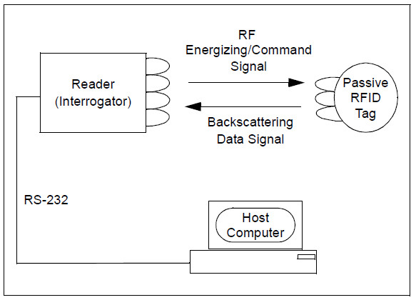
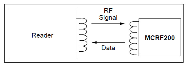
Passive RFID systems are composed of three components – a reader (interrogator), passive tag and host computer.
The tag is composed of an antenna coil and a silicon chip that includes basic modulation circuitry and non-volatile memory.
The tag is energized by a time-varying electromagnetic radio frequency (RF) wave that is transmitted by the reader.
This RF signal is called a carrier signal.
When the RF field passes through an antenna coil, there is an AC voltage generated across the coil.
This voltage is rectified to result in a DC voltage for the device operation.
The device becomes functional when the DC voltage reaches a certain level.
The information stored in the device is transmitted back to the reader.
This is often called backscattering.
By detecting the backscattering signal, the information stored in the device can be fully identified.
There are two classes of RFID device depending on type of memory cell :
(a) read only device and (b) read and write device.
The memory cell can be made of EEPROM or FRAM. EEPROM is based on CMOS silicon and FRAM is based on ferroelectric memory.
Since CMOS process technology has been matured, the EEPROM can be produced relatively at lower cost than the FRAM device.
However, FRAM based RFID device consumes less power which is desirable for low power device.
Therefore, it is known as a good candidate for the future RFID device, if its manufacturing cost becomes compatible to that of the CMOS technology.
Because of its simplicity for use, the passive RFID system has been used for many years in various RF remote sensing applications.
Specifically in access control and animal tracking applications.
In recent years, there have been dramatic increases in application demands. In most cases, each applications uses a unique packaging form factor, communication protocol, frequency, etc.
Because the passive tag is remotely powered by reader’s RF signal, it deals with very small power (~ μw).
Thus, the read range (communication distance between reader and tag) is typically limited within a proximity distance.
The read range varies with design parameters such as
frequency, RF power level, reader’s receiving sensitivity, size of antenna, data rate, communication protocol, current consumptions of the silicon device, etc.
Low frequency bands (125 kHz-400 kHz) were traditionally used in RFID applications. This was because of the availability of silicon devices.
Typical carrier frequency (reader’s transmitting frequency) in today’s applications range from 125 kHz-2.4 GHz.
In recent years, the applications with high frequency (4-20 MHz) and microwave (2.45 GHz) bands have risen with the advent of new silicon devices.
Each frequency band has advantages and disadvantages.
The 4-20 MHz frequency bands offer the advantages of low (125 kHz) frequency and microwave (2.4 GHz) bands.
Therefore, this frequency band becomes the most dominant frequency band in passive RFID applications.
FIGURE 1: SIMPLE CONFIGURATION OF RFID SYSTEMS
MODULATION PROTOCOL
The passive RFID tag uses backscattering of the carrier frequency for sending data from the tag to reader.
The amplitude of backscattering signal is modulated with modulation data of the tag device.
The modulation data can be encoded in the form of ASK (NRZ or Manchester), FSK or PSK.
Therefore, the modulation signal from the tag is Amplitude-Amplitude, Amplitude-FSK and Amplitude-PSK.
See MicroID 125 kHz Design Guide for Amplitude, Amplitude-FSK and Amplitude-PSK reader.
CARRIER
Carrier is the transmitting radio frequency of reader (interrogator).
This RF carrier provides energy to the tag device, and is used to detect modulation data from the tag using backscattering.
In read/write device, the carrier is also used to deliver interrogator’s command and data to the tag.
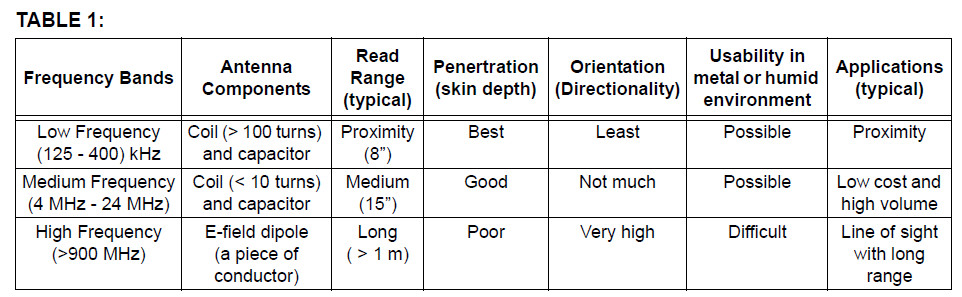
Typical passive RFID carrier frequencies are:
a) 125 kHz-400 kHz
b) 4 MHz-24 MHz
c) 900 MHz-2.45 GHz.
The frequency bands must be selected carefully for applications because each one has its own advantages and disadvantages.
Table 1 shows the characteristic of each frequency bands.
BACKSCATTER MODULATION
This terminology refers to the communication method used by a passive RFID tag to send data to the reader using the same reader’s carrier signal.
The incoming RF carrier signal to the tag is transmitted back to the reader with tag’s data.
The RF voltage induced in the tag’s antenna is amplitude- modulated by the modulation signal (data) of tag device.
This amplitude-modulation can be achieved by using a modulation transistor across the LC resonant circuit or partially across the resonant circuit.
The changes in the voltage amplitude of tag’s antenna can affect on the voltage of the reader antenna.
By monitoring the changes in the reader antenna voltage (due to the tag’s modulation data), the data in the tag can be reconstructed.
The RF voltage link between reader and tag antennas are often compared to a weakly coupled transformer coils;
as the secondary winding (tag coil) is momentarily shunted, the primary winding (reader coil) experiences a momentary voltage drop.
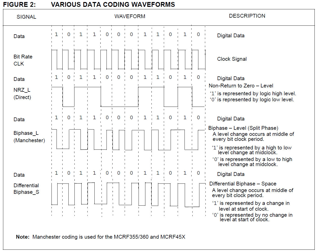
DATA ENCODING
Data encoding refers to processing or altering the data bitstream in-between the time it is retrieved from the RFID chip’s data array and its transmission back to the reader.
The various encoding algorithms affect error recovery, cost of implementation, bandwidth, synchronization capability and other aspects of the system design.
Entire textbooks are written on the subject, but there are several popular methods used in RFID tagging today:
1. NRZ (Non-Return to Zero) Direct.
In this method no data encoding is done at all; the 1’s and 0’s are clocked from the data array directly to the output transistor.
A low in the peak-detected modulation is a ‘0’ and a high is a ‘1’.
2. Differential Biphase.
Several different forms of differential biphase are used, but in general the bitstream being clocked out of the data array is modified
so that a transition always occurs on every clock edge, and 1’s and 0’s are distinguished by the transitions within the middle of the clock period.
This method is used to embed clocking information to help synchronize the reader to the bitstream.
Because it always has a transition at a clock edge, it inherently provides some error correction capability.
Any clock edge that does not contain a transition in the data stream is in error and can be used to reconstruct the data.
3. Biphase_L (Manchester).
This is a variation of biphase encoding in which there is not always a transition at the clock edge.
The MCRF355/360 and MCRF45X devices use this encoding method.
DATA MODULATION FOR 125 kHz DEVICES (MCRF2XX)
Although all the data is transferred to the host by amplitude-modulating the carrier (backscatter modulation),
the actual modulation of 1’s and 0’s is accomplished with three additional modulation methods:
1. Direct.
In direct modulation, the Amplitude Modulation of the backscatter approach is the only modulation used.
A high in the envelope is a ‘1’ and a low is a ‘0’. Direct modulation can provide a high data rate but low noise immunity.
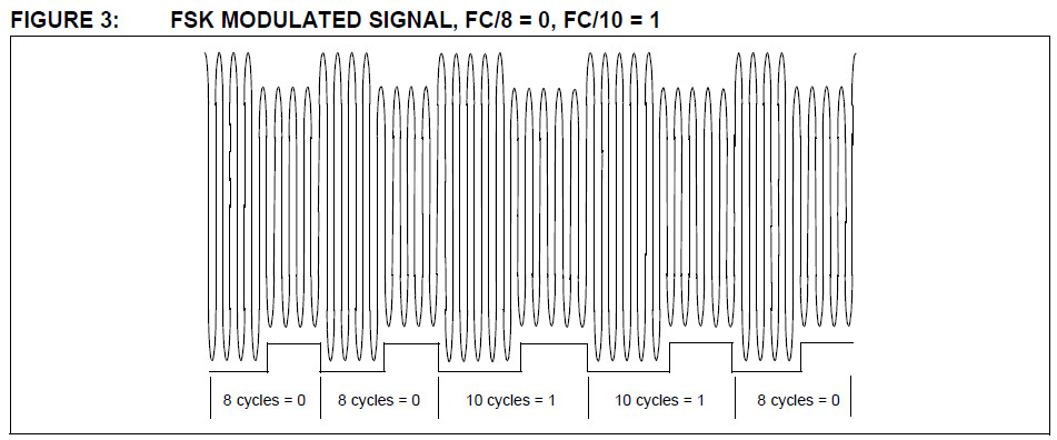
2. FSK (Frequency Shift Keying).
This form of modulation uses two different frequencies for data transfer; the most common FSK mode is FC/8/10.
In other words, a ‘0’ is transmitted as an amplitude-modulated clock cycle with period corresponding to the carrier frequency divided by 8,
and a ‘1’ is transmitted as an amplitude-modulated clock cycle period corresponding to the carrier frequency divided by 10.
The amplitude modulation of the carrier thus switches from FC/8 to FC/10 corresponding to 0’s and 1’s in the bitstream,
and the reader has only to count cycles between the peak-detected clock edges to decode the data.
FSK allows for a simple reader design, provides very strong noise immunity, but suffers from a lower data rate than some other forms of data modulation.
In Figure 3, FSK data modulation is used with NRZ encoding.
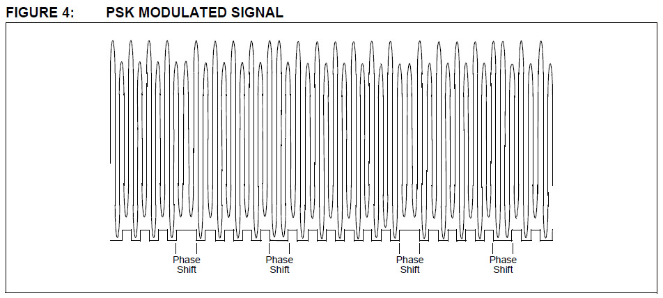
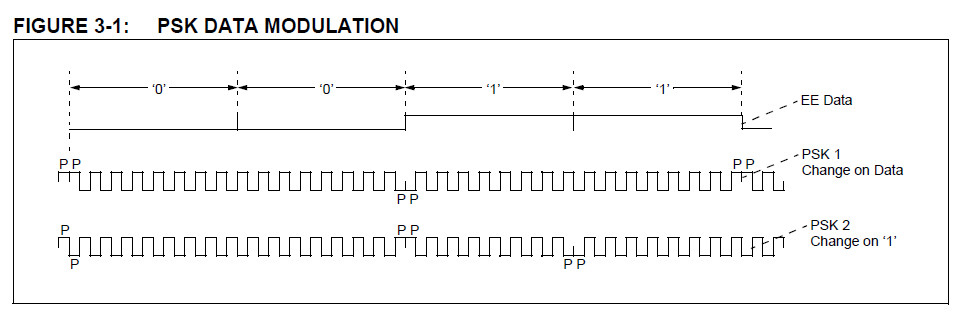
3. PSK (Phase Shift Keying).
This method of data modulation is similar to FSK, except only one frequency is used, and
the shift between 1’s and 0’s is accomplished by shifting the phase of the backscatter clock by 180 degrees.
Two common types of PSK are:
• Change phase at any ‘0’, or
• Change phase at any data change (0 to 1 or 1 to 0).
PSK provides fairly good noise immunity, a moderately simple reader design, and a faster data rate than FSK.
Typical applications utilize a backscatter clock of FC/2, as shown in Figure 4.
MCRF200 125 kHz microID Passive RFID Device
Features:
• Factory programming and memory serialization (SQTPSM)
• One-time contactless programmable (developer kit only)
• Read-only data transmission after programming
• 96 or 128 bits of One-Time Programmable (OTP) user memory (also supports 48 and 64-bit protocols)
• Typical operation frequency: 100 kHz-400 kHz
• Ultra low-power operation (5 μA @ VCC = 2V)
• Modulation options: - ASK, FSK, PSK
• Data Encoding options: - NRZ Direct, Differential Biphase, Manchester Biphase
• Die, wafer, COB, PDIP or SOIC package options
• Factory programming options
2.1 RF Front-End
The RF front-end of the device includes circuits for rectification of the carrier, VDD (operating voltage) and high-voltage clamping.
This section also includes a clock generator and modulation circuit.
2.1.1 RECTIFIER – AC CLAMP
The rectifier circuit rectifies RF voltage on the external LC antenna circuit.
Any excessive voltage on the tuned circuit is clamped by the internal circuitry to a safe level to prevent damage to the IC.
2.1.2 POWER-ON RESET
This circuit generates a Power-on Reset when the tag first enters the reader field.
The Reset releases when sufficient power has developed on the VDD regulator to allow correct operation.
2.1.3 CLOCK GENERATOR
This circuit generates a clock based on the carrier frequency from the reader.
This clock is used to derive all timing in the device, including the baud rate and modulation rate.
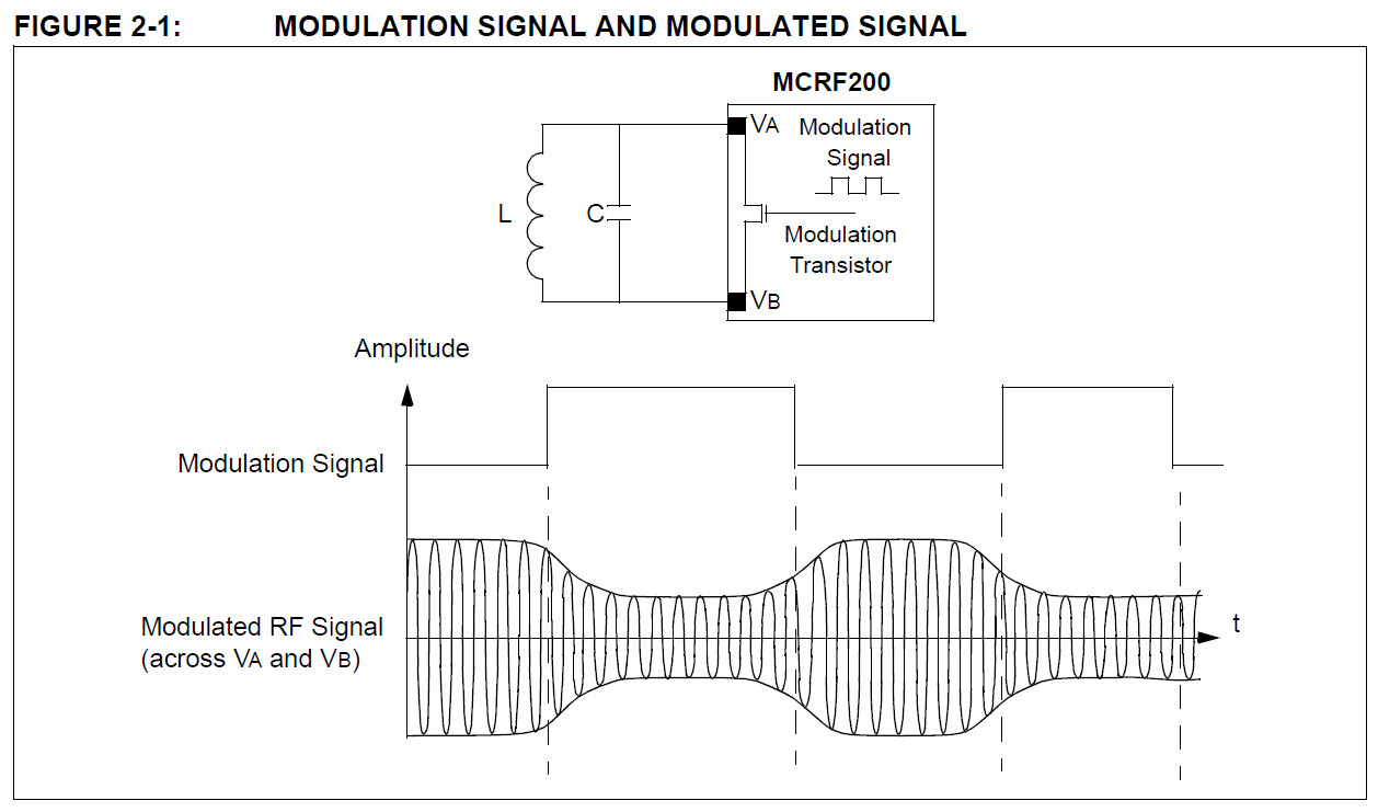
2.1.4 MODULATION CIRCUIT
The device sends the encoded data to the reader by AM-modulating the coil voltage across the tuned LC circuit.
A modulation transistor is placed between the two antenna coil pads (VA and VB).
The transistor turns on and off based on the modulation signal.
As a result, the amplitude of the antenna coil voltage varies with the modulation signal. See Figure 2-1 for details.
2.2 Configuration Register and Control Logic
The configuration register determines the operational parameters of the device.
The configuration register can not be programmed contactlessly; it is programmed during wafer probe at the Microchip factory.
CB11 is always a zero; CB12 is set when successful contact or contactless programming of the data array has been completed.
Once CB12 is set, device programming and erasing is disabled. Table 2-4 contains a description of the bit functions of the control register.
2.2.1 BAUD RATE TIMING OPTION
The chip will access data at a baud rate determined by bits CB2, CB3 and CB4 of the configuration register.
For example, MOD32 (CB2 = 0, CB3 = 1, CB4 = 1) has 32 RF cycles per bit. This gives the data rate of 4 kHz for the RF carrier frequency of 128 kHz.
The default timing is MOD128 (FCLK/128), and this mode is used for contact and contactless programming.
Once the array is successfully programmed, the lock bit CB12 is set. When the lock bit is set, programming and erasing the device becomes permanently disabled.
The configuration register has no effect on device timing until the EEPROM data array is programmed (CB12 = 1).
2.2.2 DATA ENCODING OPTION
This logic acts upon the serial data being read from the EEPROM.
The logic encodes the data according to the configuration bits CB6 and CB7.
CB6 and CB7 determine the data encoding method.
The available choices are:
• Non-return to zero-level (NRZ_L) -- Direct
• Biphase_S -- Differential
• Biphase_L -- Manchester
• Inverted Manchester ( Biphase_L )
2.2.3 MODULATION OPTION
CB8 and CB9 determine the modulation protocol of the encoded data. The available choices are:
• ASK
• FSK
• PSK_1
• PSK_2
When ASK (direct) option is chosen, the encoded data is fed into the modulation transistor without change.
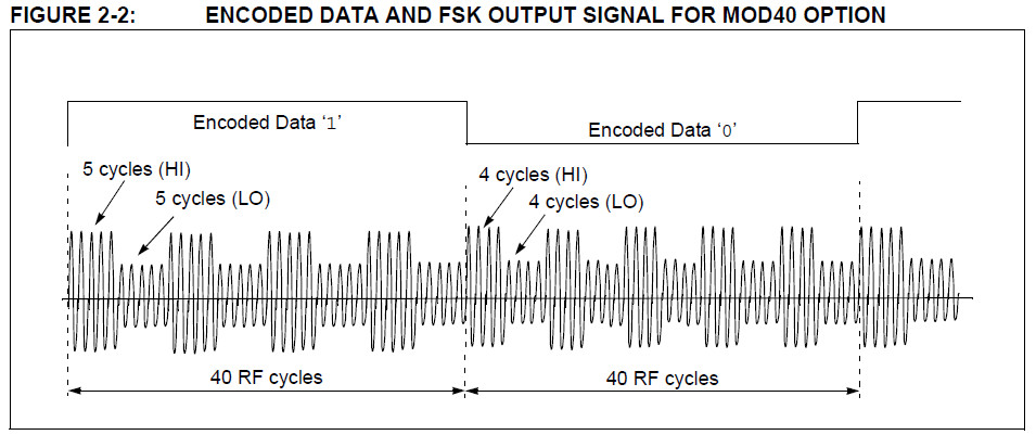
When FSK option is chosen, the encoded data is represented by:
a) Sets of 10 RF carrier cycles (first 5 cycles →higher amplitude, the last 5 cycles → lower amplitude) for logic “high” level.
b) Sets of 8 RF carrier cycles (first 4 cycles →higher amplitude, the last 4 cycles → lower amplitude) for logic “low” level.
For example, FSK signal for MOD40 is represented:
a) 4 sets of 10 RF carrier cycles for data ‘1’.
b) 5 sets of 8 RF carrier cycles for data ‘0’.
Refer to Figure 2-2 for the FSK signal with MOD40 option.
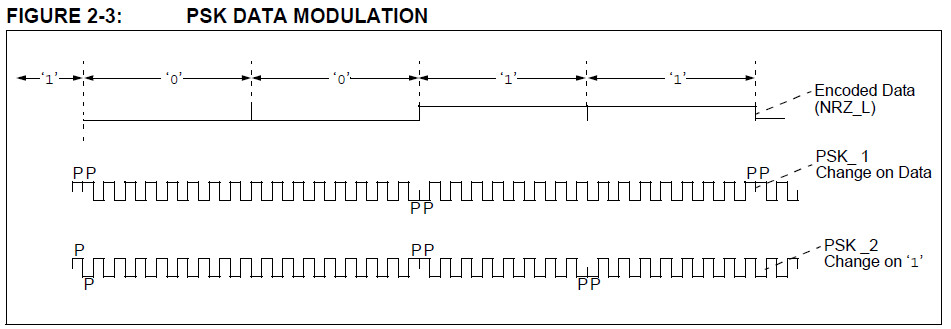
The PSK_1 represents change in the phase of the modulation signal at the change of the encoded data.
For example, the phase changes when the encoded data is changed from ‘1’ to ‘0’, or from ‘0’ to ‘1’.
The PSK_2 represents change in the phase at the change on ‘1’.
For example, the phase changes when the encoded data is changed from ‘0’ to ‘1’, or from ‘1’ to ‘1’.
FSK Reader Reference Design
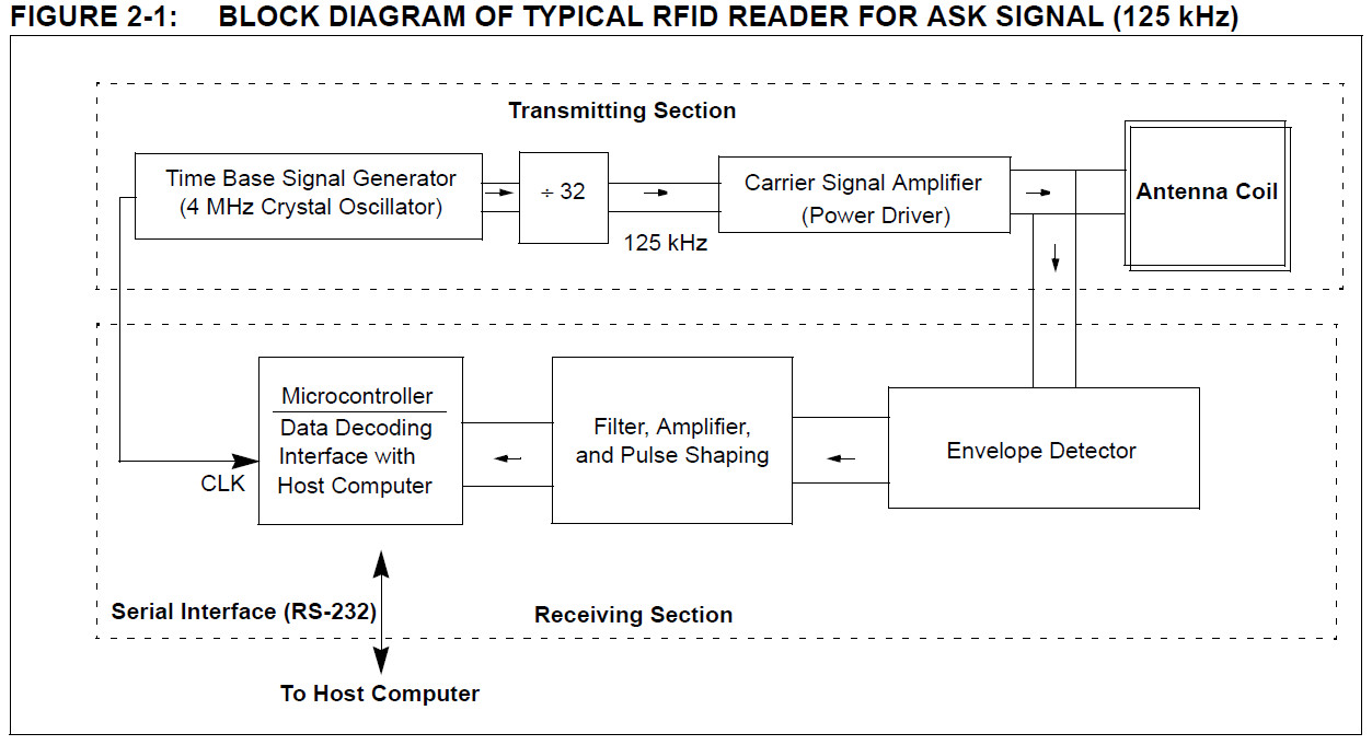
2.1 Transmitting Section
The transmitting section contains circuitry for a carrier signal (125 kHz), power amplifiers, and a tuned antenna coil.
The 125 kHz carrier signal is typically generated by dividing a 4 MHz (4 MHz/32 = 125 kHz) crystal oscillator signal.
The signal is amplified before it is fed into the antenna tuning circuit.
A complementary power amplifier circuit is typically used to boost the transmitting signal level.
An antenna impedance tuning circuit consisting of capacitors is used to maximize the signal level at the carrier frequency.
This tuning circuit is also needed to form an exact LC resonant circuit for the carrier signal.
The tuning compensates the variations in the component values and the perturbation of coil inductance due to environment effect.
A design guide for the antenna coil is given in AN710, Antenna Circuit Design for RFID Applications (DS00710).
2.1.1 LIMITS ON TRANSMITTING SIGNAL LEVEL (FCC PART 15) IN THE USA
Each country limits the signal strength of the RF wave that is intentionally radiated by a device.
In the USA, the signal strength of the carrier signal (125 kHz) radiating from the antenna coil must comply with the FCC (Federal Communications Commission) part 15 regulation.
The signal level is specified by the 47 CFR Part 15.209a of the federal regulation.
For a 125 kHz signal, the FCC limits the signal level to 19.2 μv per meter, or 25.66 dBμV (i.e., 20 log(19.2) = 25.66 dBμV), at 300 meters away from the antenna.
For a close distance measurement, an extrapolation rule (40 dB per decade) is applied (Part 15.31.f.2). For example, the signal level at 30 meters away from the device must not exceed:
25.66 dBμV + 40 dBμV = 65.66 dBμV
2.2 Receiving Section
The receiving section consists of an antenna coil, demodulator, filters, amplifiers, and microcontroller.
In applications for close proximity read range, a single coil is often used for both transmitting and receiving.
For long read-range applications, however, separated antennas may be used.
More details on the antenna coil are given in AN710, Antenna Circuit Design for RFID Applications (DS00710).
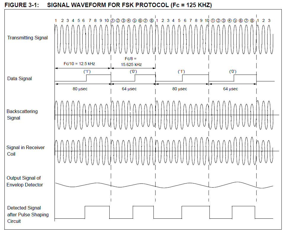
In the FSK communication protocol, a ‘0’ and a ‘1’ are represented by two different frequencies.
In the MCRF200, a ‘0’ and a ‘1’ are represented by Fc/8 and Fc/10, respectively. Fc is the carrier frequency.
The MCRF200 sends this FSK signal to the reader by an amplitude modulation of the carrier signal.
The FSK reader needs two steps for a full recovery of the data.
The first step is demodulating the backscattering signal, and the second step is detecting the frequency (or period) of the demodulation signal.
The demodulation is accomplished by detecting the envelope of the carrier signal.
A half-wave capacitor-filtered rectifier circuit is used for the demodulation process.
A diode detects the peak voltage of the backscattering signal.
The voltage is then fed into an RC charging/discharging circuit.
The RC time constant must be small enough to allow the voltage across C to fall fast enough to keep in step with the envelope.
However, the time constant must not be so small as to introduce excessive ripple.
The demodulated signal must then pass through a filter and signal shaping circuit before it is fed to the microcontroller.
The microcontroller performs data decoding and communicates with the host computer through an RS-232 or other serial interface protocols.
3.0 microID FSK READER
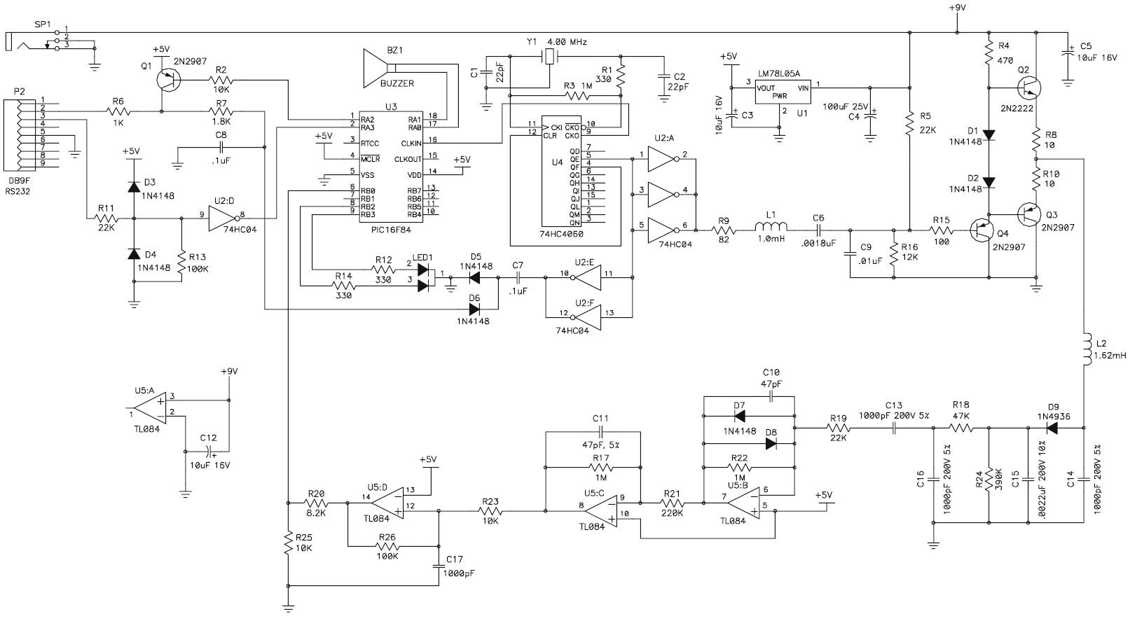
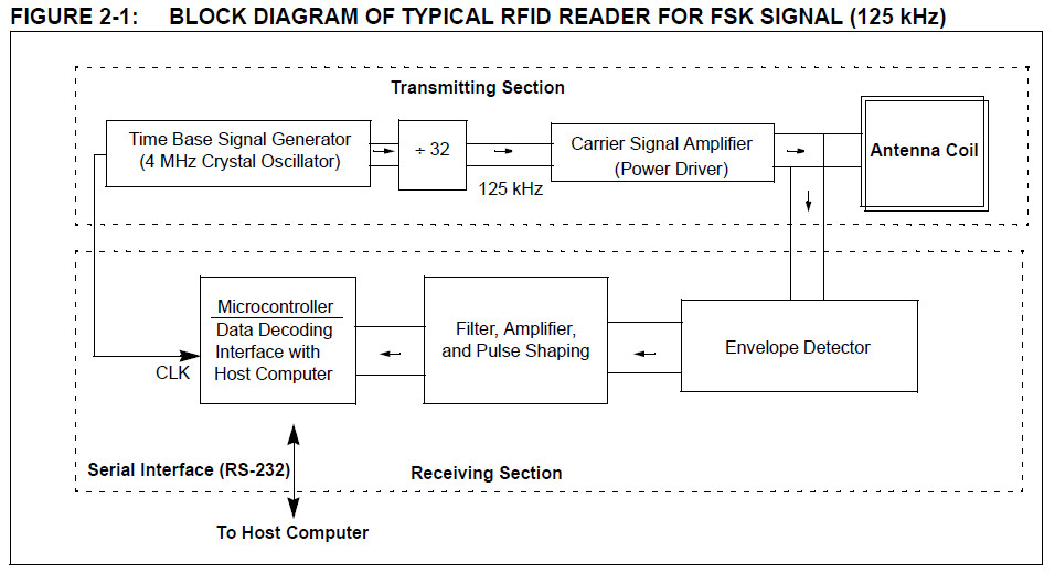
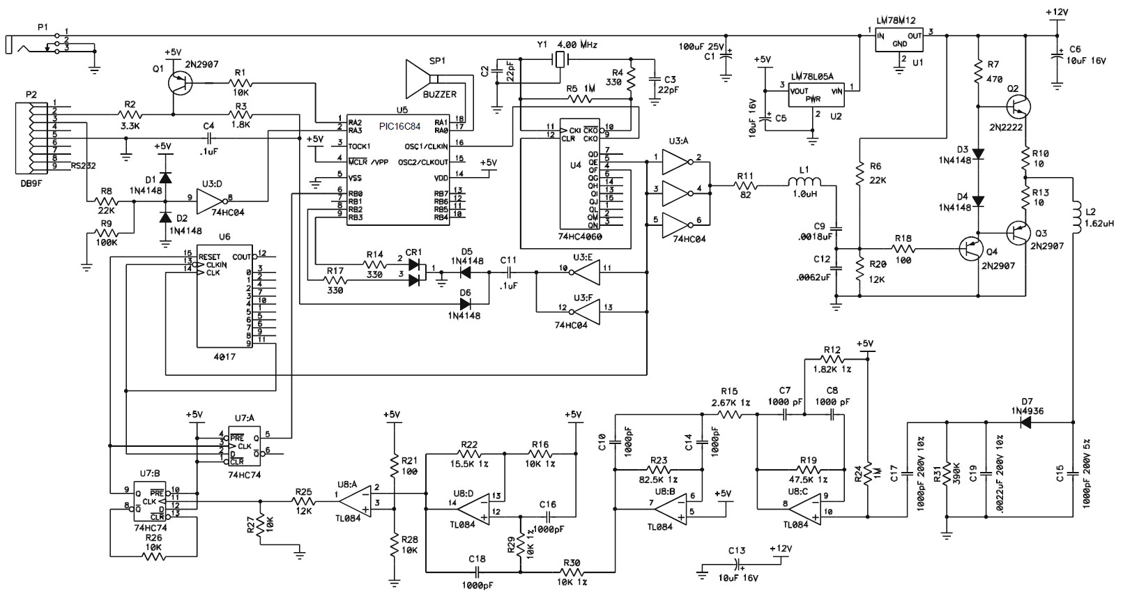
The electronic circuitry for an FSK reader is shown in Figure 3-1.
The reader needs +9 VDC power supply.
The 125 kHz carrier signal is generated by dividing the 4 MHz time base signal that is generated by a crystal oscillator.
A 16-stage binary ripple counter (74HC4060) is used for this purpose. The 74HC4060 also provides a clock signal for the PIC16C84 microcontroller.
The 125 kHz signal is passed to an RF choke (L1) and filter before it is fed into a power amplifier that is formed by a pair of complementary bipolar transistors (Q2 and Q3).
For long read-range applications, this power amplifier circuit can be modified.
Power MOSFETs may be used instead of the bipolar transistors (2N2222). These power MOSFETs can be driven by +24 VDC power supply.
A push-pull predriver can be added at the front of the complementary circuit. This modification will enhance the signal level of the carrier signal.
The reader circuit uses a single coil for both transmitting and receiving signals.
An antenna coil (L2: 1.62 mH) and a resonant capacitor (C2: 1000 pF) forms a series resonant circuit for a 125 kHz resonance frequency.
Since the C2 is grounded, the carrier signal (125 kHz) is filtered out to ground after passing the antenna coil.
The circuit provides a minimum impedance at the resonance frequency.
This results in maximizing the antenna current, and therefore, the magnetic field strength is maximized.
L2, C15, D7, and the other bottom parts in the circuit form a signal receiving section.
The voltage drop in theantenna coil is a summation (superposition) of transmitting signal and backscattering signal.
The D7 is a demodulator which detects the envelope of the backscattering signal.
The FSK signal waveforms are shown in Figure 3-1.
D7 and C19 form a half-wave capacitor-filtered rectifier circuit.
The detected envelope signal is charged into the C19.
R21 provides a discharge path for the voltage charged in the C19.
This voltage passes active filters (U8) and the pulse shaping circuitry (U8) before it is fed into the PIC16C84 for data processing.
The PIC16C84 microcontroller performs data decoding and communicates with the host computer via an RS-232 serial interface.
PSK Reader Reference Design
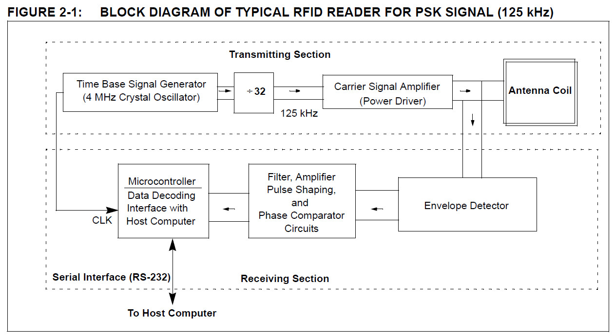
2.1 Transmitting Section
The transmitting section contains circuitry for a carrier signal (125 kHz), power amplifiers, and a tuned antenna coil.
The 125 kHz carrier signal is typically generated by dividing a 4 MHz (4 MHz/32 = 125 kHz) crystal oscillator signal.
The signal is amplified before it is fed into the antenna tuning circuit. A complementary power amplifier circuit is typically used to boost the transmitting signal level.
An antenna impedance tuning circuit consisting of capacitors is used to maximize the signal level at the carrier frequency.
This tuning circuit is needed to form an exact LC resonant circuit for the carrier signal.
The tuning compensates the variations in the component values and the perturbation of coil inductance due to environment effect.
A design guide for the antenna coil is given in AN710, Antenna Circuit Design for RFID Applications (DS00710).
2.2 Receiving Section
The receiving section consists of an antenna coil, demodulator, filter, amplifier, pulse shaping, phase comparator, and microcontroller.
In applications for proximity read-range, a single coil is often used for both transmitting and receiving.
For long read range application, however, separated antennas may be used.
More details on the antenna coil are given in AN710, Antenna Circuit Design for RFID Applications (DS00710).
In the PSK communication protocol, the phase of the modulation signal changes with the data.
Two most common types of phase encoding method are:
(a) change phase at any data change (‘0’ to ‘1’ or ‘1’ to ‘0’), and
(b) change phase at ‘1’.
A typical data rate for PSK applications is one half of the carrier frequency, and it is faster than FSK.
However, it requires a wider bandwidth than FSK.
The PSK reader needs two steps for a full recovery of the data.
The first step is demodulating the backscattering signal, and
the second step is detecting the phase changes in the demodulation signal.
The demodulation is accomplished by detecting the envelope of the carrier signal.
A full-wave capacitor-filtered rectifier circuit is used for the demodulation process.
A diode detects the peak voltage of the backscattering signal.
The voltage is then fed into an RC charging/discharging circuit.
The RC time constant must be small enough to allow the voltage across C to fall fast enough to keep in step with the envelope.
However, the time constant must not be so small as to introduce excessive ripple.
The demodulated signal must then pass through a filter, an amplifier, signal shaping, and phase comparator circuits before it is fed to the microcontroller.
The microcontroller performs data decoding and communicates with the host computer through an RS-232 or other serial interface protocols.
3.0 microID PSK READER
The MCRF200 can be configured with either PSK_1 or PSK_2 modulation.
he PSK_1 changes the phase of the modulation signal on any change of the data (i.e., 0 to 1 or 1 to 0).
The PSK_2 changes the phase of the modulation signal on the first clock edge of a data ‘1’.
Figure 3-1 shows the optional PSK encoding protocols.
The PSK encoded data is amplitude modulating the carrier signal.
A typical PSK modulated signal is shown in Figure 3 in AN680, Passive RFID Basics page 6.
This reference reader was designed for use with an MCRF200 with 08Dh in its configuration register, which represents
PSK_1, NRZ Direct, Fc/32, data rate, and 128 bits.
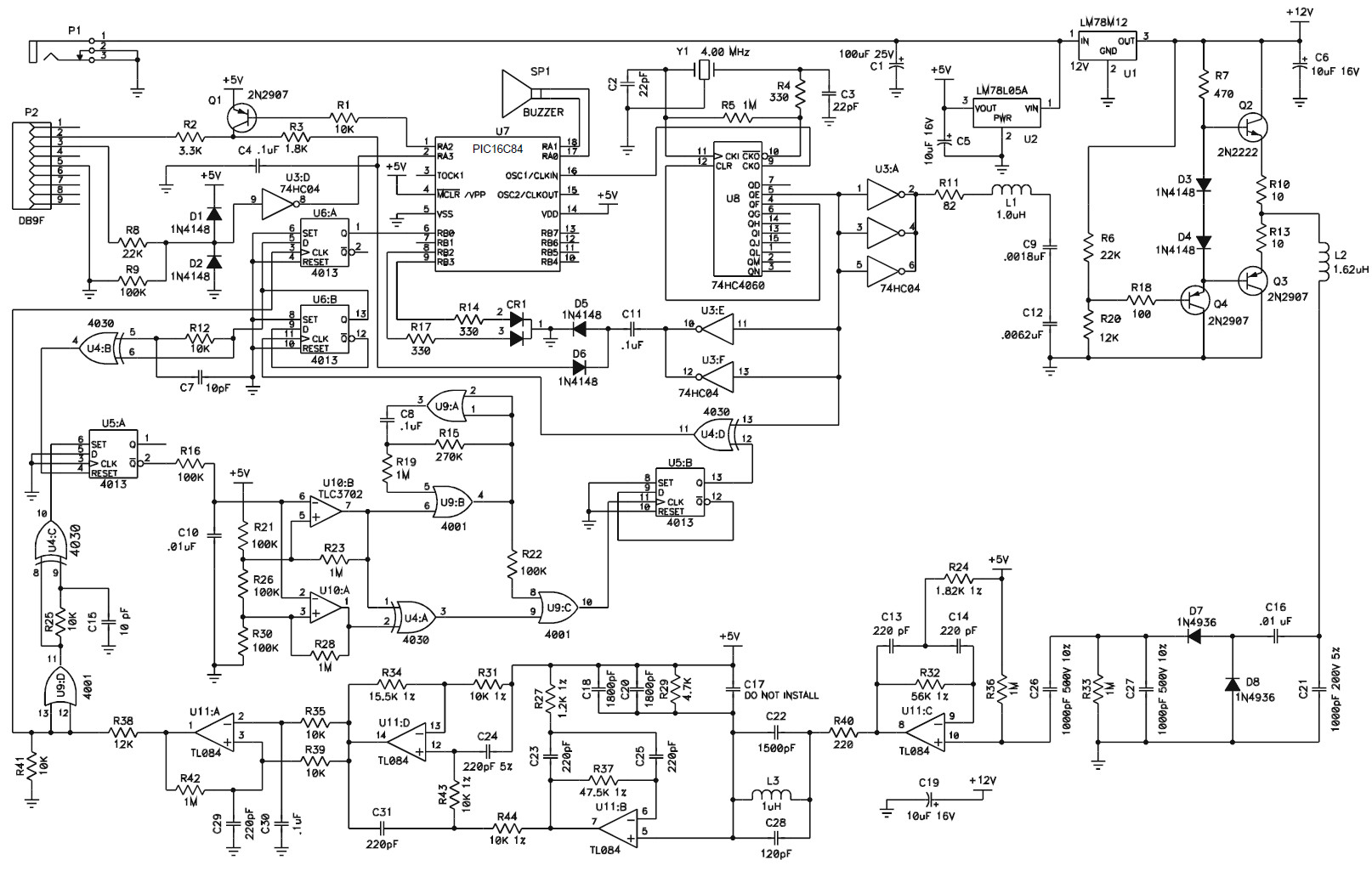
The electronic circuitry for the PSK reader is shown in Figure 3-1.
The reader needs +9 to +15 VDC power supply.
The 125 kHz carrier signal is generated by dividing the 4 MHz time-base signal that is generated by a crystal oscillator.
A 16-stage binary ripple counter (74HC4060) is used for this purpose. The 74HC4060 also provides a clock signal for the PIC16C84 microcontroller.
Signal from the U8 is also used as a phase reference for receiving signals.
The 125 kHz signal is passed to an RF choke (L1) and filter before it is fed into a power amplifier that is formed by a pair of complementary bipolar transistors (Q2 and Q3).
For long read-range applications, this power amplifier circuit can be modified. Power MOSFETs may be used instead of bipolar transistors (2N2222).
These power MOSFETs can be driven by +24 VDC power supply. A push-pull predriver can be added at the front of the complementary circuit.
This modification will enhance the signal level of the carrier signal.
The reader circuit uses a single coil for both transmitting and receiving signals.
An antenna coil (L2: 1.62 mH) and a resonant capacitor (C21: 1000 pF) forms a series resonant circuit for 125 kHz resonance frequency.
Since the C21 is grounded, the carrier signal (125 kHz) is filtered out to the ground after passing the antenna coil.
The circuit provides minimum impedance at the resonance frequency.
This results in maximizing the antenna current, and therefore, the magnetic field strength is maximized.
In the circuit, D7 and D8 are amplitude demodulators that are detecting the envelope of the backscattering signal.
D7 provides a current path during a positive half cycle and the D8 during the negative half cycle.
The detected envelope signal is charged into the C27.
A discharge path for the voltage charged in the C27 is provided by R33.
This voltage passes active filters (U11:C) and the pulse shaping circuitry (U11:A).
The output from the U11 is a square wave at 62.5 kHz, which exhibits 180 degree phase-shifts in accordance with changes in the data stream from the tag.
This signal is used as a clock for D flip-flop (U6:A) for which the D input is a reference 62.5 kHz square wave derived from the 125 kHz transmitting signal.
As the phase of the received signal changes, the output of the flip-flop changes, based on whether the clocking occurs during the high or low portions of the reference signal.
The recovered data signal is fed to the input I/O pin of the PICmicro MCU (U7) for decoding.
One of the major problems encountered with the PSK reader is that the phase of the returned signal with respect to a reference signal is, for several reasons, indeterminate.
If the transitions of the incoming signal and the reference are occurring at the same time, the output of the D flip-flop will be unpredictable.
To guarantee that this does not happen, additional circuits have been added.
The received 62.5 kHz signal is buffered by U9:D and a pulse is generated upon every transition of the received signal by U4:C.
Likewise, U4:B provides a string of pulses on every transition of the reference 62.5 kHz signal.
Note that these pulse strings are at 125 kHz and are independent of the phase state of the received signal.
These pulses are fed to the set and reset lines of U5:A and result in a 125 kHz output at Q whose duty cycle is proportional to the phase difference between the two pulse signals.
If the duty cycle is near 50%, then the transitions of the 62.5 kHz signals are approximately 90 degrees different which is ideal for PSK demodulation.
R6 and C10 filter the output of U5:A resulting in a DC level proportional to the phase shift. This level is the input to a window detector consisting of U10 and U4:A.
If the DC level is near the midpoint, the output of comparator U10:B would be high and the output of comparator U10:A would be low.
Therefore, the output of U4:A would be high. If the DC level is higher than the reference level set by R21, R26, and R30 then the outputs of both comparators would be high,
resulting in a low output from U4:A. Similarly, if the DC level is low, both outputs would be low, which would also result in a low output at U4:A.
Note that the 125 kHz signal from which the 62.5 kHz reference is obtained passes through gate U4:D.
A change of the state on the control output to this gate allows the 125 kHz signal to be 180 degree phase-shifted.
This results in a phase-shift in the 62.5 kHz reference of 90 degrees. If the output of the U9:C is low, the flip-flop U5:B will maintain its current state.
If the output of U4:A goes low, which would signify an undesirable phase relationship between the 62.5 kHz signals, then the output of U9:C would have a transition to high, causing U5:B to change state.
This would change the reference phase 90 degrees, thus bringing the phases of the 62.5 kHz signals back into a desirable relationship and return the output of U4:A to a high state.
In the event that no tag is present, Q of U5:A is always high which makes the output of U10:B low. This turns on an oscillator consisting of U9:A, U9:B, C8, R15, and R19.
This oscillator toggles U5:B at about 200 Hz, allowing the reader to be looking for a tag signal with both reference signal phases.
When a good tag signal appears, the circuit locks on in a good phase relationship and demodulates the incoming 62.5 kHz signal.
As the tag comes closer to the reader, the phase will be shift for a number of reasons.
If the shift is sufficient, the reference signal will shift as necessary to maintain good demodulation.
The PIC16C84 microcontroller performs data decoding and communicates with host computer via an RS-232 serial interface.
ASK Reader Reference Design