1.1 


1.2 


1.3 


1.4 


1.5 

2. Single-Stage CMOS Amplifiers
2.1.1 CS Stage with Ideal Current-Source Load


2.1.2 CS Stage with Current-Source Load


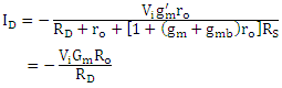
2.1.3 CS Stage with Degeneration

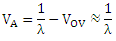
A. 
加 设电流为,或着在drain terminal加看电压
 ,即可算出
,即可算出


B. 
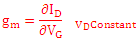
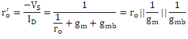
一个网络的 即为他的输入电压
 所驱动的向外界提供的电流
 ,或是从外界抽取的电流
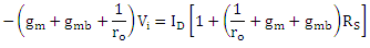
 。所以针对研究
 的等效电路其"外界"应用一根接地的短路导线表示,因为此时体现
 驱动力的电流
 ,全部都集中在了这一根短路导线上,而不可能出现在任何有阻支路上。

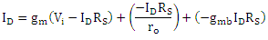


这说明了下图中左边两种组态都可化简成右边图所示的小信号模型。

C. 


2.1.4 CS Stage with Diode-Connected Load


2.2 CG Stage
2.2.1 CG Stage with Ideal Current-Source Load

A. 

B. 

C. 


2.2.2 CG Stage with Resistive Load and Impedance of Signal Source

A. 

B. 


这种现象同样可以用2.1.3 B中的方法进行理解。
C. 


2.3 Source Follower: CD Stage
2.3.1 CD Stage with Ideal Current-Source Load

A. 

B. 

C. 


2.3.1 CD Stage with Resistive Load and Drain Resistor

A. 


B. 

C. 

2.4 Cascode Stage

A. 


B. 

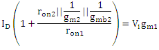

C. 
