最近在用Arria10。从480降到270的过程中,IOPLL出现问题,大概是说几个Bank的IOPLL已经被占用,没有空间再给别的IOPLL去适配。
因为在工程中,所用的PLL多达35个之多,其中明确为自己手动例化的IOPLL为8个,DDR占用3个Bank所以也会占用3个IOPLL。
一时之间不知道从哪里下手,于是笔者理了下思路,觉得应该搞明白Arria10 PLL的分布,果不其然,收获颇多。
以下主要以Arria10 270为例。
首先要搞清楚的是Arria10中的PLL共有多少个,分别分布在什么位置。从图1看GX270的有8个IOPLL和8个fPLL。从图2和图4可以看到
GX270共有8个IO Bank和4个高速接口Bank。从图3和图5可以看到一个IO Bank有一个IOPLL,一个高速接口Bank有2个fPLL和个ATX PLL(有待研究)。

图1

图2

图3

图4
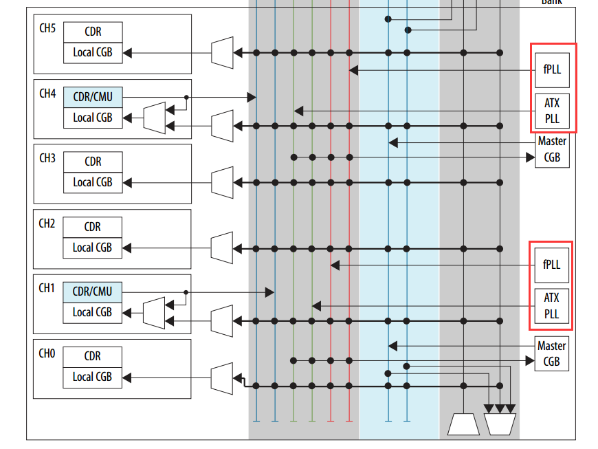
图5
那现在的问题是我已经使用了11个IOPLL,是否可以把部分IOPLL转成fPLL呢?接下下要了解下PLL的特征:
(1)The fPLLs are located adjacent to the transceiver blocks in the HSSI banks. Each HSSI
bank contains two fPLLs. You can configure each fPLL independently in conventional
integer mode or fractional mode.
(2)The fPLL and I/O PLL clock outputs can drive all clock networks.
(3)The dedicated clock input pins can be either differential clocks or single-ended clocks
for I/O PLL. When you use the dedicated clock input pins as single-ended clock inputs,
only CLK_[2,3][A..L]_[0,1][p,n]pins have dedicated connections to the PLL.
fPLLs only support differential clock inputs.
(4)The I/O PLLs are located adjacent to the hard memory controllers and LVDS serializer/
deserializer (SERDES) blocks in the I/O banks. Each I/O bank contains one I/O PLL.
从以上几个特征来看,fPLL完全可以实现IOPLL的所有功能,只是在输入上要保证必须为差分。
在工程中一个HSSI Bank有两输入部分,每一部分要用到一个fPLL,刚好可以,但是例外的是有一个Bank还有一个输出部分,也要用一个fPLL.
一个HSSI Bank中的fPLL有两个,如果在这个Bank中要使用到两个以上的fPLL应该怎么办呢?这里也引出一个问题,是不同的HSSI Bank之间的fPLL能否共用?
很幸运,笔者很快从Arria10 Transciver PHY User Giude中找到了3.2.4 Reference Clock Network部分,内容如下:
The reference clock network distributes a reference clock source to either the entire
left or right side of the FPGA where the transceivers reside. This allows any reference
clock pin to drive any transmitter PLL on the same side of the device. Designs using
multiple transmitter PLLs which require the same reference clock frequency and are
located along the same side of the device, can share the same dedicated reference
clock (refclk) pin
很明显,在同一个Block中的fpLL可以被任一个参考时钟所驱动。