advanced packaging
Here we take a look at some of the strategies that enable next-generation advanced packaging, including wafer-level packaging, bumping, redistribution layers, fan out, and through-silicon vias. These are great examples of applying front-end wafer manufacturing technologies (such as deposition, etch, and clean) to back-end processing.
在这里,我们将探讨实现下一代高级封装的一些策略,包括晶圆级封装,凸点,重新分布层,扇出和硅通孔。这些都是将前端晶圆制造技术(例如沉积,蚀刻和清洁)应用于后端处理的绝佳示例。
Wafer-Level Packaging
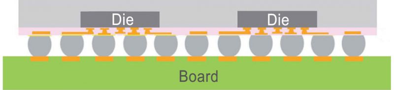
In conventional packaging, the finished wafer is cut up, or diced, into individual chips, which are then bonded and encapsulated. Wafer-level packaging (WLP), as its name implies, involves packaging the die while it is still on the wafer: protective layers may be bonded to the top and/or bottom of the wafer, then electrical connections are prepared and the wafer is diced into individual chips. To provide a baking analogy, traditional packaging is similar to frosting individual cupcakes, while WLP is like frosting a whole cake and then slicing it into pieces. Because the sides are not coated with WLP, the resulting packaged chip is small in size (roughly the same size as the chip itself), an important consideration in footprint-sensitive devices such as our smartphones. Other advantages include streamlined manufacturing and the ability to test chip functionality before dicing.
在常规包装中,将完成的晶片切割或切成单个芯片,然后将其粘合和封装。顾名思义,晶圆级封装(WLP)涉及在裸片仍在晶圆上时对其进行封装:可以将保护层粘合到晶圆的顶部和/或底部,然后准备电连接,并制备晶圆。切成单个芯片。为了提供类似的烘焙效果,传统的包装类似于给单个纸杯蛋糕上糖霜,而WLP就像是先将整个蛋糕上糖霜然后切成小块。由于侧面未涂WLP,因此封装后的芯片尺寸较小(与芯片本身的尺寸大致相同),这是对足迹敏感型设备(例如我们的智能手机)的重要考虑因素。

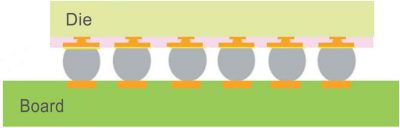
Bumping and Flip Chips
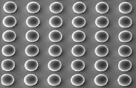
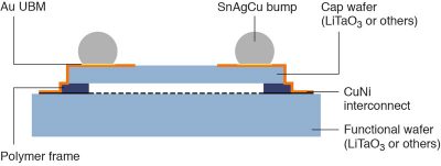
One of the simplest electrical connections between a chip and the circuit board can be made with small balls of electrically conductive material, called bumps. A bumped die can then be flipped upside down and aligned so that the bumps connect with matching pads on the board. Flip chip bonding has several advantages over traditional wire bonding, including small package size and greater device speed.
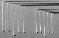
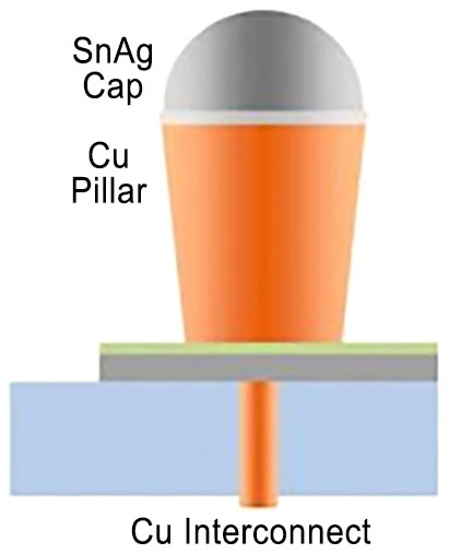
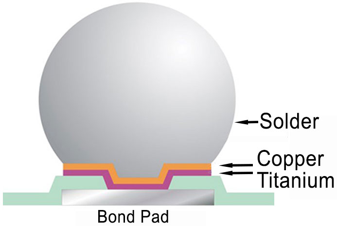
Bumping can be performed by extending conventional wafer fabrication methods. After the chips are made, underbump metallization (UBM) pads are created to connect to the chip circuitry, and bumps are then deposited on the pads. Solder is the most commonly used bumping material, although alternative materials – such as gold, copper, or cobalt – can also be used depending on the application. For high-density interconnects or fine-pitch applications, copper pillars can be used. While solder bumps spread during the joining process, copper pillars retain their shape, which allows them to be placed much more closely together.
凸块和倒装芯片芯片和电路板之间最简单的电连接之一可以由称为凸块的小导电材料球制成。然后可以将颠倒的管芯上下颠倒并对齐,以使颠簸与板上的匹配焊盘相连。与传统的引线键合相比,倒装芯片键合具有多个优势,包括较小的封装尺寸和更高的器件速度。
可以通过扩展常规的晶片制造方法来执行凸块。制作完芯片后,会创建凸块下金属化(UBM)焊盘以连接到芯片电路,然后在焊盘上沉积凸点。焊料是最常用的凸点材料,尽管根据应用场合也可以使用其他材料,例如金,铜或钴。对于高密度互连或细间距应用,可以使用铜柱。尽管在连接过程中焊料凸块扩散,但铜柱仍保持其形状,这使它们可以更紧密地放置在一起。

Redistribution Layers
Relocating, or redistributing, contact points is another technology that can be done efficiently at the wafer level. A redistribution layer (RDL) is used to reroute connections to desired locations. For example, a bump array located in the center of a chip can be redistributed to positions near the chip edge. The ability to redistribute points can enable higher contact density and enable subsequent packaging steps. This “fan-in” process also creates one of the smallest packages available.
The redistribution process adds another set of layers over the wafer surface. A dielectric film is deposited for electrical isolation, then the original bond pads are exposed. Metal lines are deposited to relocate the pads to desired locations, and underbump metallization layers are built to support the solder (or other metal) bumps.
重新
分布层重新定位或重新分布接触点是另一种可以在晶圆级高效完成的技术。重新分配层(RDL)用于将连接重新路由到所需位置。例如,位于芯片中心的凸块阵列可以重新分配到靠近芯片边缘的位置。重新分配点的能力可以实现更高的接触密度并实现后续的封装步骤。此“扇入”过程还会创建可用的最小软件包之一。
重新分配过程在晶片表面上添加了另一组层。沉积电介质膜以进行电隔离,然后暴露原始的焊盘。沉积金属线以将焊盘重新定位到所需位置,并构建凸块下金属化层以支撑焊料(或其他金属)凸块。

Fan-Out WLP
The redistribution process can also be used to spread or “fan out” the connection points. This may be needed, for example, when the chip shrinks in size while requiring the same number of contact points. One solution is to fan out the contacts beyond the dimensions of the chip. A compelling application of this technology is the improved electrical and thermal performance along with a reduction in overall package height.
Fan-out wafer-level packaging (FOWLP) typically involves first dicing the front-end-processed wafer into individual die. These die are then spaced apart on a carrier structure, and the gaps are filled in to form a reconstituted wafer. Once the artificial wafer has been built, the contacts can be redistributed beyond the perimeter of the original die using WLP processing.
扇出WLP重
分布过程也可以用于扩展或“扇出”连接点。例如,当芯片尺寸缩小而需要相同数量的接触点时,可能需要这样做。一种解决方案是将触点扩展到芯片尺寸之外。该技术的一项引人注目的应用是改善了电气和热性能,并降低了整体封装高度。
扇出晶圆级封装(FOWLP)通常涉及首先将经过前端处理的晶圆切成单个裸片。然后将这些管芯在载体结构上隔开,并填充间隙以形成重构晶片。一旦构建了人造晶圆,就可以使用WLP处理将触点重新分布到原始管芯的外围。

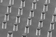
Through-Silicon Vias
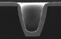
While bumping and RDL may reduce the surface area chips use on a circuit board, space usage can be even more efficient when chips are stacked. Even better, stacking is a strategy that improves the electrical performance of multiple chips. Wire bonding is one way to create stacked assemblies, and silicon vias (TSVs) have emerged as an attractive alternative that can offer a smaller form factor. A TSV is an electrical connection through the entire thickness of the chip, creating the shortest possible path from one side of the chip to the other. The short interconnect length between chips can also mean lower power consumption and greater bandwidth.
In one common way to create TSVs, the vias (holes) are etched from the front side of the wafer to a certain depth. These are then isolated and filled by depositing a conductive material, typically copper. After chip fabrication is complete, the wafer is thinned from the back side to expose the vias, and metal is deposited on the backside of the wafer to complete the TSV interconnection.
硅通孔
虽然凸点和RDL可以减少芯片在电路板上的表面积,但在堆叠芯片时,空间利用率甚至可以更高。更好的是,堆叠是提高多个芯片电气性能的策略。引线键合是创建堆叠组件的一种方法,而硅通孔(TSV)已成为一种有吸引力的替代方法,可以提供更小的尺寸。TSV是贯穿芯片整个厚度的电连接,可形成从芯片一侧到另一侧的最短路径。芯片之间的互连长度短也意味着更低的功耗和更大的带宽。
在一种常见的创建TSV的方式中,从晶圆的正面将通孔(孔)蚀刻到一定深度。然后通过沉积导电材料(通常为铜)将其隔离并填充。芯片制造完成后,将晶圆从背面减薄以暴露通孔,并在晶圆的背面沉积金属以完成TSV互连。

Packaging Technology Evolution
No longer an afterthought in the semiconductor manufacturing process, packaging has exploded with innovation and complexity. In particular, wafer-level packaging has experienced tremendous advancements in materials, processes, and equipment, enabling WLP to become one of the fastest growing chip packaging technologies. Bumping, redistribution layers, fan out, through-silicon vias, and other techniques have contributed to the small-form-factor chips with powerful, high-speed functionality that we consumers expect in our mobile electronics. We look forward to seeing the next generation of semiconductor devices enabled by leading-edge packaging technologies.
封装技术的发展封装
不再是半导体制造过程中的事后思考,其创新和复杂性已经爆炸式增长。特别地,晶圆级封装在材料,工艺和设备方面经历了巨大的进步,使WLP成为发展最快的芯片封装技术之一。凸点,重新分布层,扇出,硅通孔以及其他技术已为我们的消费者提供了希望在移动电子产品中具有强大,高速功能的小尺寸芯片。我们期待看到由领先的封装技术支持的下一代半导体器件。
ASM NEXX
ASMPT完成收購NEXX 準備就緒迎接先進半導體封裝之高速增長
新加坡,香港, 2018年10月2日 - (亞太商訊) - 全球最大之半導體裝嵌及包裝設備供應商ASM Pacific Technology Limited (「ASMPT」/ 「集團」) 公布於二零一八年十月一日完成向Tokyo Electron Limited (「TEL」) 收購TEL NEXX, Inc (「NEXX」) 的交易。TEL NEXX將被納入ASMPT的後工序設備分部。 是次收購標誌著ASMPT踏出推行其策略的重要一步,進軍新的高增長市場,並擴大產品種類至先進半導體封裝市場。
NEXX成立於二零零一年,為先進封裝市場的領導者,在高度專業的電化學沉積 (ECD) 和物理氣相沉積 (PVD) 技術方面具有強大的技術能力。透過NEXX的技術與ASMPT的廣泛產品種類及全球支援的結合,集團將能夠擴大其業務組合及繼續向客戶提供最創新的解決方案。
ASMPT行政總裁李偉光先生表示:「在收購TEL NEXX後,ASMPT將具有獨特的定位,成為能夠為封裝及表面貼裝市場分部提供一站式互聯解決方案的綜合『互聯』公司。我們現在能夠在業內提供更廣泛的互聯解決方案組合,包括引線焊接、覆晶、熱壓焊接,加上NEXX的 PVD 及 ECD 設備,集團更能夠提供包括凸塊底層金屬(UBM)、銅柱 (微間距銅柱)、矽穿孔(TSV)及重布層 (RDL) 等等的互聯解決方案。」
於收歸ASMPT旗下後的全新NEXX結構中,Tom Walsh將留任ASM NEXX總裁,他將向後工序設備業務分部副行政總裁CK Lim匯報。
關於 ASM Pacific Technology Limited 作爲全球科技及市場領導者,ASMPT (香港聯交所股份代號: 0522) 致力為全球半導體裝嵌及封裝行業研發及提供尖端解決方案及物料。其表面貼裝技術解決方案廣泛應用於不同的終端用戶市場,包括一般電子產品、移動通信器材、汽車工業、工業、LED以及替代能源。集團持續投資於研究及發展,為集團客戶提供創新及具有成本效益的解決方案和系統,以協助他們提升生產效率、可靠性及產品的質量。 ASMPT自一九八九年起於香港聯交所上市。目前,ASMPT已獲納入為恒生綜合市值指數下之恒生綜合中型股指數、恒生綜合行業指數下之恒生綜合資訊科技業指數、恒生香港35指數及恒生環球綜合指數的成份股。詳細資訊請查閱ASMPT網頁 www.asmpacific.com 。
Intro
ASM NEXX, Inc. provides our customers with the on substrate results they require using our high technology capital equipment for advanced packaging electrochemical deposition 电化学沉积 and physical vapor deposition物理气相沉积 (ECD and PVD). Our team of experts will work with your production team to qualify processes in the areas of:
- Wafer Level Packaging
- Bumping (Cu Pillar and SnAg)
- Redistribution layers (Au and Cu RDL)
- Fan Out
- RF Filters SAW and BAW
- Panel Level Plating
- Power Devices
- 2.5D/3D TSV
- EMI Shielding
- TSV
ASM NEXX,Inc.使用我们的高科技资本设备,为客户提供其先进的电化学沉积和物理气相沉积(ECD和PVD)所需的基板上结果。我们的专家团队将与您的生产团队合作,以验证以下领域的流程:
- 晶圆级包装
- 碰撞(铜柱和锡银)
- 重新分配层(Au和Cu RDL)
- 扇出
- 射频滤波器SAW和BAW
- 面板级电镀
- 电力设备
- 2.5D / 3D TSV
- EMI屏蔽
- 硅通孔
ASM NEXX,Inc.开发了高级功能,可以支持生产线中端的特定高级包装市场,无论是在工厂还是在装配厂。这些独特的创新解决方案使我们的客户群能够实现当今世界上最精确的电镀和溅射性能,同时将生产率保持在比其他供应商高出2倍和3倍的水平,从而创造了无与伦比的价值主张。
ASM NEXX, Inc. has developed advanced features and capabilities to support specific Advanced Packaging Markets in the middle end of the line, whether in the fab or at the assembly house. These unique innovative solutions enable our customer base to achieve some the most accurate plating and sputtering performance in the world today while maintaining productivity rates 2X and 3X higher than alternative suppliers, resulting in a value proposition that is second to none.
Bumping
Bumping is an advanced wafer level process technology where “bumps” or “balls” made of various metals are formed on the substrate before the wafer or board is cut, or “diced” into individual chips. Wafer bumping is an essential part of flip chip or board level semiconductor packaging which has become the standard in interconnect technology in consumer electronics today. These “bumps” are the components that connect the die to the substrate and become the package after singulation. These interconnect building blocks can be bumps or copper pillars, composed of metal solders, such as eutectic or lead free SnAg.
凸块是一种先进的晶圆级处理技术,其中在将晶圆或板切割或“切块”成单个芯片之前,在基板上形成由各种金属制成的“凸块”或“球”。晶圆隆起是倒装芯片或板级半导体封装的重要组成部分,倒装芯片或板级半导体封装已成为当今消费电子产品中互连技术的标准。这些“凸块”是将管芯连接到基板并在分割后成为封装的组件。这些互连构建块可以是由金属焊料(例如共晶或无铅SnAg)组成的凸块或铜柱。
The bumps, or pillars, provide shorter pathways than wire bonds between die and substrate to improve the electrical, mechanical and thermal performance of the flip chip package. For the performance driven market, flip chip interconnects reduce signal propagation delay, provide better bandwidths, and relieve the constraints of power distribution. Bump composition and dimension depends on requirements such as final form factor, cost and the electrical, mechanical and thermal performance. Cu Pillar structures have become the interconnect solution of choice for fine pitch, lead-free, or high current application devices. For the form factor driven market, such as mobile applications, replacing wire bonding by flip chip interconnects reduces the size and weight of the package as well as delivering better performance.
与裸片和衬底之间的引线键合相比,凸块或支柱提供的路径更短,从而改善了倒装芯片封装的电气,机械和热性能。对于性能驱动的市场,倒装芯片互连可减少信号传播延迟,提供更好的带宽并减轻配电的限制。凸块的组成和尺寸取决于最终形状因数,成本以及电气,机械和热性能等要求。铜柱结构已成为小间距,无铅或大电流应用设备的互连解决方案。对于诸如移动应用之类的尺寸驱动市场,用倒装芯片互连代替引线键合可以减小封装的尺寸和重量,并提供更好的性能。
 来源:先进封装的系列报告**YoleDéveloppement公司,2018 www.i-micronews.com
Cu Pillar
Bumps

RDL

Via Fill
产品供应
ASM NEXX提供了专门用于凸点工艺的溅射和电镀晶圆级以及电镀面板级解决方案。NEXX还提供了其他功能和选项,以支持当今已知的过程和未来的变化,随着互连技术的成熟,这些变化和变化不可避免。NEXX服务于新兴市场的大批量生产领域。
ASM NEXX offers sputtering and plating wafer level and plating panel level solutions dedicated to the bumping process. NEXX also offers additional features and options to support today’s known processes and future variations that inevitably evolve as the interconnect technologies mature. NEXX serves the high volume production segment of the bumping market.
晶圆溅镀– Apollo 300

Apollo Under Bump Metallization(UBM)是一种在线物理气相沉积系统,适用于制造具有多种高级包装功能(例如一系列铜再分布层(RDL))的客户,Apollo UBM可生产最紧凑的厚膜和薄膜在市场上的足迹。
Apollo Under Bump Metallization (UBM) is an in-line physical vapor deposition system for customers who manufacture multiple advanced packaging features, such as a range of copper redistribution layers (RDL), the Apollo UBM produces both thick and thin films in the most compact footprint on the market.
好处
-
适用于厚膜和薄膜的高通量溅射解决方案
-
应力管理可减少晶圆和芯片翘曲
-
处理多种晶圆尺寸
-
更安全地处理多种晶片类型
-
High throughput sputtering solution for thick and thin films
-
Stress management to reduce wafer and die warpage
-
Handles multiple wafer sizes
-
Safer handling of an array of wafer types
-
多达5种不同的金属
-
德加斯
-
直流脉冲溅射
-
背气(BSG)
-
反应溅射
-
射频偏置
-
ICP和CCP蚀刻
-
静电夹头
-
桥接工具功能
-
完全可配置
-
处理300和200毫米晶圆
200 -
Up to 5 different metals
-
Degas
-
DC Pulsed Sputtering
-
Backside Gas (BSG)
-
Reactive Sputtering
-
RF Bias
-
ICP and CCP etch
-
Electrostatic chucks
-
Bridge tool capability
-
Fully configurable
-
Processes 300 and 200 mm wafers
200
晶圆电镀– Stratus TM P300
对于制造多个高级封装功能(包括标准铜柱互连和微型凸点)的客户。P300的高速晶圆处理系统可提供灵活性和可扩展性,以生产大型和小型特征。
- 市场上生产率最高的电镀工具
- 用一个工具处理RDL,铜柱和TSV
- 处理多种晶圆尺寸
- 更安全地处理多种晶片类型
- 屏蔽层使更快的镀覆成为可能,同时保持良好的晶片内均匀度
特征
- 多达6种不同的化学物质
- 用于高容量或低容量电镀的各种储液罐尺寸化学稳定池技术(SnAg和Ni)
- ShearPlate技术
- 多达30个晶圆处理
- 桥接工具功能
- 完全可配置
- 处理300和200毫米晶圆
相关产品:S300,S200
面板电镀– Stratus TM P500
事实证明,StratusTM P500可在领先的面板制造商提供高达510 x 515毫米的面板上提供晶圆级电镀精度。这种面板规模的电镀工具是半导体行业的变革者,因为它为玻璃和环氧面板基板带来了更高质量的晶圆级化学物质。
好处
- 市场上技术含量最高的面板电镀工具,可提供<10 um RDL L / S和一系列高级封装功能
- 更安全地处理薄,弯曲和翘曲的面板
- 屏蔽层可加快电镀速度,同时保持良好的面板内均匀度
特征
- 多达5种不同的化学物质
- 高容量或低容量镀膜的各种储液罐尺寸
- ShearPlate技术
- 分段阳极
- 单面或双面电镀
- 桥接工具功能
- 完全可配置
- 处理510 x 515毫米面板
Fan out
The Fan Out process generally represents the redistribution of the interconnects located inside and outside of the die envelope. The term fan out often includes a variety of assembly methods: embedded wafer level package (WLP), embedded wafer level ball grid array (eWLB), wafer level system in package (WLSiP). The Fan Out process can also embed chip capacitors and inductors and has also been contemplated for 3D die stacking.
扇出过程通常表示位于管芯封套内部和外部的互连的重新分布。扇出一词通常包括多种组装方法:嵌入式晶圆级封装(WLP),嵌入式晶圆级球栅阵列(eWLB),晶圆级封装中系统(WLSiP)。扇出工艺还可以嵌入芯片电容器和电感器,并且也已考虑用于3D芯片堆叠。
The Fan Out technology is often a process of reconstituting a new wafer or panel on all KGD (known good die). KGD are accurately placed and temporarily held on to an interposer with double sided sticky tape or an adhesive. Then, EMC (Embedded Mold Compound) is applied to create a new wafer or panel. Once the new wafer or panel is created then the front-end lithography steppers apply the RDL (Redistribution Layer) connecting and relocating the interconnections. The RDL process demands that increasingly thin PVD seeds be sputtered and finer RDLs be plated with micron accuracy and tight uniformity over the entire wafer or panel substrate. One of the major challenges is finding sputtering and plating machines that can deliver thin, uniform seeds and fine line RDL plating below 10 um L/S uniformly across a variety of large areas.
扇出技术通常是在所有KGD(已知良好管芯)上重新构造新晶圆或面板的过程。将KGD准确放置并用双面胶带或粘合剂暂时固定在插入器上。然后,应用EMC(嵌入式模塑料)来创建新的晶圆或面板。一旦创建了新的晶圆或面板,前端光刻步进器就会应用RDL(重新分布层)来连接并重新定位互连。RDL工艺要求溅射出越来越薄的PVD种子,并以微米精度和紧密均匀性在整个晶圆或面板基板上电镀更细的RDL。主要的挑战之一是找到一种溅射和电镀机,该设备可以在各种大面积上均匀地提供厚度小于10 um L / S的薄而均匀的种子和细线RDL电镀。
 来源:先进封装的系列报告YoleDéveloppement公司,2018 www.i-micronews.com
铜柱 Cu Pillar
颠簸 Bumps
RDL
宏铜柱 Macro Cu Pillar
产品供应
ASM NEXX提供专门用于FanOut工艺的溅射和电镀晶圆级以及电镀面板级解决方案。NEXX还提供了其他功能和选项,以支持当今已知的过程和将来的变化,随着扇出过程的成熟,这些变化不可避免地会演变。NEXX服务于FanOut市场的大批量生产领域。
RF filter
As mobile handsets reach a greater portion of the earth’s population, the need for radio spectrums to communicate these devices to one another has skyrocketed. Five bands at the turn of the century has increased to more than 30 as we approach the 5G communication standard slated for 2020. Radio frequency (RF) front end modules and filters are key components to enabling 5G networks as 5G communication protocols are defined and implemented. RF and microwave filters represent a class of electronic filter, designed to operate on signals in the megahertz to gigahertz frequency ranges (medium frequency to extremely high frequency).
随着移动电话覆盖地球人口的更大比例,对无线电频谱将这些设备相互通信的需求激增。随着我们接近2020年制定的5G通信标准,世纪之交的五个频段已增加到30多个。随着定义和实施5G通信协议,射频(RF)前端模块和滤波器是启用5G网络的关键组件。 。射频和微波滤波器代表一类电子滤波器,旨在对兆赫兹至千兆赫兹频率范围(中频至极高频)的信号进行操作。
Acoustic wave technology, such as the popular Surface Acoustic Wave filter (SAW) and the higher technology Bulk Acoustic Wave (BAW) filter for more challenging interference environments, deliver interdigital transducers (IDTs) that provide some of the highest performance, smallest and lowest-cost filters in analog RF communication. Different filters trap acoustic energy in different ways. Manufacturers are increasingly coupling filters with amplifiers or an array of other devices to achieve even smaller form factors and higher functionality in the end package. The challenge for filter manufacturers is to safely plate and sputter metals on a variety of very fragile, small wafer sizes.
声波技术,例如流行的表面声波滤波器(SAW)和技术更先进的体声波(BAW)滤波器,可用于更具挑战性的干扰环境,它们提供叉指换能器(IDT),这些叉指换能器可提供某些性能最高,体积最小和成本最低的传感器,模拟RF通信中的成本过滤器。不同的滤波器以不同的方式捕获声能。制造商越来越多地将滤波器与放大器或其他设备阵列耦合在一起,以在最终封装中实现更小的外形尺寸和更高的功能。过滤器制造商面临的挑战是如何在各种非常脆弱的小晶圆尺寸上安全地电镀和溅射金属。
Download
Product Brochure Chinese (PDF)
Product Offering
ASM NEXX offers sputtering and plating wafer level and plating panel level solutions dedicated to the RF Filters processes. NEXX also offers additional features and options to support today’s known process and future variations that inevitably evolve as the RF Filters process matures. NEXX serves the high volume production segment of the RF Filters market.
ASM NEXX提供专用于RF滤波器工艺的溅射和电镀晶圆级以及电镀面板级解决方案。NEXX还提供了其他功能和选项,以支持当今已知的过程和未来的变化,随着RF滤波器过程的成熟,这些变化不可避免地会演变。NEXX服务于RF滤波器市场的大批量生产领域。
Amicra
新加坡与香港,2018年4月3 日 – ASM Pacific Technology Ltd(「ASMPT」)宣布已完成收购AMICRA Microtechnologies GmbH(「Amicra」)100%的股份。 Amicra为光电子和先进封装市场的高精密固晶机主要供应商。这项于2018年4月4日完成的交易将加强公司业务,不仅能够为快速发展的矽光电子组装设备市场提供服务,还能够服务更高精度的覆晶和固晶市场。
总部位于新加坡,并在香港联交所上市的ASMPT是全球最大的后工序半导体设备供应商和SMT解决方案提供商。 ASMPT将把Amicra重新命名为ASM AMICRA Microtechnologies GmbH,并将Amicra合并到ASMPT的后工序设备业务分部。
ASMPT集团行政总裁李伟光表示:「我们对这一战略投资感到非常兴奋。 Amicra的亚微米高精度贴片机补充了集团现有的产品组合。 Amicra在光电子市场中占有领先地位,而集团认为该市场具有高增长潜力。我相信这次合并将进一步加强我们未来的发展机遇,并为我们的客户提供更高的附加价值。」
「随着我们对高精度固晶市场的渗透日益增加,特别是在矽光电子制造业,与强大的战略合作伙伴进行合并可以更好地支持我们不断增长的国际客户基础。凭借其规模、已建立的国际供应链、销售渠道和客户支援能力,与ASMPT的合并将使我们能够进一步发展业务。我为Amicra和我们的客户感到高兴,亦很高兴有机会与ASMPT合作。」Amicra董事总经理Rudolf Kaiser说。
狂砸81亿港元,TCL为什么要打ASM太平洋的主意?
手机报在线 · 手机报在线·2018-10-09 09:47
![]() 3.2k
3.2k
有外媒报道,知情人士称,TCL集团正与顾问探索收购ASMI所持有的ASMPT,即ASM太平洋25%股权的可能性。据外媒测算,按9月28日的收盘价计算,这部分股权价值约81亿港元。9月28日收盘时ASM太平洋股价上涨0.13%至79.7港元,总市值约322.33亿港元。

ASM Pacific Technology Ltd.(简称ASMPT)是全球最大的半导体和发光二极管行业的集成和封装设备供应商。成立于1975年,为跨国芯片制造商,独立 集成电路 (IC)装配工厂和 消费电子 产品制造商提供半导管装配设备及材料(蚀刻式和衡压式引线框架)。ASMPT于1989年在香港上市,目前其52.59%的股份由ASM International N.V.(简称ASMI)所持有,而ASM International N.V.是纳斯达克榜上有名的晶圆工艺处理设备提供商。
ASMPT的总部设在中国香港特别行政区,但是却同时在中国深圳,新加坡和马来西亚拥有生产和研发基地。全球并无其他设备供应商拥有类似的全面产品组合及对装嵌及SMT程序的广泛知识及经验。
从ASMPT主要的业务在 电子元器件 的后段模组封装设备领域,包括LED光源、LCD\OLED显示屏SMT及连接、芯片支架封装及SMT等,另外,ASMPT除了提供摄像头模组的芯片支架封装及SMT设备与材料外,还是业内主要的“AA”制程设备供应商。
手机报在线与ASMPT有着长期的合作关系,在近两年手机报在线为行业推广先进的摄像头生产制程、全面屏显示技术先进制程的各种主题活动中,ASMPT都为行业带来了最前沿的技术动态与先进工艺制程分享,为推动中国内地的3D/双摄摄像头技术进步与产能提升,全面屏COF\COG先进制程的普及与产能提升,做出了重要的贡献。
从ASMPT2018年的半年报中我们可以看到,受益于后工序设备分部、物料分部、SMT解决方案三大业务较去年同期分别增长14.4%、12.1%、24.6%,上半年的收入为96.16亿港元,较2017年同期增长17.48%;毛利为39.12亿港元,同比增长17.97%。但由于所得税开支同比增长115.27%,导致持有人应占溢利下滑6%至13.97亿港元。其中后工序设备分部的增长,主要依靠CIS市场对ASM主动式镜头对位”AA”设备的强劲需求。SMT解决方案分部收入的提升,则依赖汽车及 工业电子 市场,并得益于国内手机供应链市场占有率的扩大。
另外,还在四月份与东电电子(TOKYO ELECTRON LTD)达成了收购其美国子公司TEL NEXX的协议,下半年获得主管部门批准后,ASMPT将在 芯片封装 技术上得到ECD和PVD两项RDL关键技术,以应对10纳米以下制程封装市场需要。
不过由于全球的半导体投资速度趁缓,中国内地手机市场低迷,行业产能过剩状况也越来越严重,外界投资者对ASMPT的前景预期并不乐观,其股价目前也处于相对的低位。相比去年底高点时的127.58港元,ASMPT股价已经下跌了37.5%,或许这也是TCL想在低位的时候出手的原因之一。
目前TCL集团的传统业务的盈利能力已经不敌其华星光电的面板业务,而在最新的全面屏显示技术上,ASMPT是业内除了三星与JDI两家的合作供应商外,少有能提供COF与COP后段模组封装技术的厂商。今年苹果发布的新机,其OLED显示屏模组就是采用COP封装,LCD显示屏模组则采用了COF封装。
另外,TCL集团虽然说不会主动投资芯片生产制造企业,但却设立了半导体投资机构,希望能从资本投资的方向来让集团获取收益。这样一来,对于TCL集团希望取得类似ASMPT这种行业比较稀缺的上市公司股份或控制权,就一点都不意外了。
ref: