主要参考了https://www.eefocus.com/liu1teng/blog/12-02/237897_4533d.html 、Xilinx UG471、UG472以及Xilinx Forum上的一些问答,在此一并表示感谢。
------------------------------------------------------------------------------------------------------
本文主要用来随意记录一下最近在为手头的FPGA项目做约束文件时候遇到的一点关于FPGA专用时钟管脚相关的内容,意在梳理思路、保存学习结果、以供自己日后以及他人参考。
起因是在做约束文件中的时序例外约束部分的内容的时候,发现很多单位之前的FPGA项目中的约束文件里经常出现的一句时序例外约束是:
set_property CLOCK_DEDICATED_ROUTE FALSE [get_nets NETS_NAME_IBUF]
约束的对象往往是除了sys_clk之外的、由外部引入作为一些通信接口比如SPI或者MDIO接口的时钟管脚的IBUF线。
如果不加这个约束,执行implement的时候往往就会报error或者critical warning、内容中也会提到加上这个约束的话、就会将严重警告或者错误降级为普通warning,但是一直没搞明白这到底是怎么回事,所以这两天翻阅文档和论坛,算是弄清了个大概。
原来FPGA的管脚上有一类专用的时钟管脚、他们一般用于将外部的时钟信号引入FPGA、并在FPGA module中使用这些引入的时钟信号。但是如果设计时管脚分配没做好、或者管脚不够用了,那么就有可能将本该接入专用时钟管脚(或者叫做全局时钟管脚)的信号,接到了普通IO口上,这样只能通过添加CLOCK_DEDICETED_ROUTE FLASE绕过PAR的检查,但是没有解决根本问题。
在日常接触较多的Xilinx 7系列FPGA芯片上,Xilinx论坛上的工作人员对于这一点是这样解释的:
If you are bringing the the clock onto the device then you need to use the CCIO (Clock capable inputs) . Every 7 series FPGA has four clock-capable inputs in each bank. Two of the four are Multi-Region Clock Capable (MRCC) and the other two are Single Region Clock Capable (SRCC). These inputs are regular I/O pins with dedicated connections to internal clock resources.
也就是说,必须使用片上的MRCC或者SRCC引脚来把外部时钟信号引入FPGA、然后再在FPGA上使用这些引入的时钟。
对于这二者的含义和前后级连接,在UG472的table1-1中有详细说明:

关于这二者的区别,在xilinx forum的https://forums.xilinx.com/t5/Embedded-Processor-System-Design/MRCC-or-SRCC/m-p/787546
的下面的回答中进行了详细说明:
The clock capable pins in a 7 series FPGA serve two purposes; access to the local clocking resources and access to the global clocking resources.
If you are using the global clocking resources (BUFG, BUFH, MMCM, PLL) then the MRCC and SRCC have exactly the same capability - there is no difference between the two.
If you are using the local clocking resources (BUFR and BUFIO), then then the SRCC and MRCC can both only drive only the BUFIO and BUFR located in the same clock region. The BUFIO can then only drive the IOB flip-flops and high speed clock of the ISERDES in the same I/O bank and the BUFR can clock all the logic (except the high speed clock of the ISERDES) in the same clock region.
The only difference between the SRCC and MRCC is that the MRCC can also drive the BUFMR. The BUFMR can then drive the BUFIO/BUFR in the same clock region as well as in the clock regions above and below the MRCC. This would generally be used for "ChipSync" (source synchronous) interfaces that need to use more pins than are available in one I/O bank.
MRCCs can access multiple clock regions and the global clock tree. MRCCs function the same as SRCCs and can additionally drive multi-clock region buffers (BUFMR) to access up to three clock regions.
另外作者还提到了:
if you are forwarding clock out from the device, then you can use any regular IOs, I.e
Clock path is
Clock you want to forward -> ODDR -> OBUFDS ->Routed to any regular differential pair .
这里也就是说,如果需要将外部时钟引入FPGA、但是不会在FPGA的module内部将该信号作为时钟去使用、而只是将这个引入的时钟做一个relay或者说forward,那么就不需要将其接到MRCC/SRCC管脚(虽然这两类管脚在一般情况下、不做时钟引入的管脚的时候、也可以作为普通IO来使用)、而只用接到任何一个普通的IO即可。
这里还注意到的是、如果做时钟中继、使用的方案是选用ODDR-OBUFDS,这二者在UG471文档中有说明。
UG471-P128:
Clock Forwarding
Output DDR can forward a copy of the clock to the output. This is useful for propagating
a clock and DDR data with identical delays, and for multiple clock generation, where every
clock load has a unique clock driver. This is accomplished by tying the D1 input of the
ODDR primitive High, and the D2 input Low. Xilinx recommends using this scheme to
forward clocks from the FPGA logic to the output pins.
此外,在UG472的table2-1中,对不同应用场合下、时钟输入之后的各类BUF的连接方式进行了说明,包括各种常见的clk buffer:
clock management tiles (CMT)
Global clock buffers (BUFGCTRL, simplified as BUFG throughout this user guide).BUFGs do not belong to a clock region and can reach any clocking point on the device.
horizontal clock buffer (BUFH/BUFHCE)
clock enable circuit (BUFHCE)
I/O clock buffer (BUFIO)
regional clock buffer (BUFR)
multi-clock region buffers (BUFMR)
另外在https://www.eefocus.com/liu1teng/blog/12-02/237897_4533d.html中的博文中提到了:
输入输出的随路时钟,如果硬件上接到了普通IO上,这就有点悲剧了,尽管可以用BUFG接进全局时钟网,但是,从PAD到BUFG的输出有10ns的固有延时。这10ns无法消除,所以如果时钟频率超过20M左右时,skew会比较大。
这篇博文是2012年的,距离现在已经略久远,所以关于BUFG的延时数据、在现在看起来有点不可思议、直觉上觉得太大了点、尽管作者的这个10ns的数据包含了从pad-IBUFG(可能是IBUFG,也可能是其他)-BUFG的整个延时。查阅现在使用的xilinx 7 系列FPGA芯片的ds181手册、在Clock Buffers and Networks一小节的内容中找到了BUFG的delay,如下图所示:
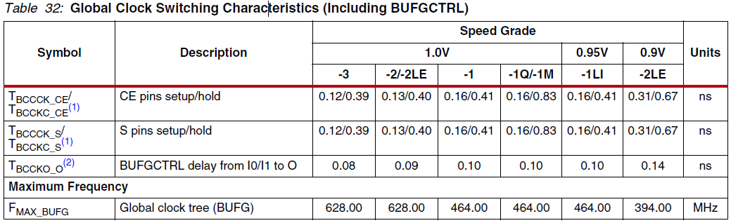
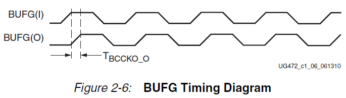
根据不同速度等级的芯片、这个延时不尽相同、大概在0.1ns左右。这里的Tbccko_o对应的就是UG472-Figure2-6中的BUFG的输入输出延时、如下图所示:
另外博文中还提到:
一些处理办法:用两个DCM级联来调相BUFG+DCM+DCM。
对应现在使用的7series FPGA中、也就是时钟BUFG+MMCM来实现时钟的相位调整。
关于DCM,MMCM和PLL的发展历史和区别,除了参阅UG472之外、在xilinx forum的回答下https://forums.xilinx.com/t5/Welcome-Join/DCM-MMCM-and-PLL/m-p/654372有详细说明:
The DCM is a Digital Clock Manager - at its heart it is a Delay Locked Loop. This has the ability to deskew a clock, generate different phases of the clock, dynamically change the phase of a clock, generate related (2x) clocks, do clock division, and even generate clocks with harmonic relationships to the incoming clock. It was the only clock management block that existed in older technologies (up to Spartan-3 and Virtex-4).
In Virtex-5 and Spartan-6 the Phase Locked Loop (PLL) was introduced along with the DCM. The PLL is an analog clock management cell that can do almost everything the DCM can do with the exception of dynamic and fine phase shifting. However, it can do more precise frequency generation and can generate multiple different frequencies at the same time. It also has significantly better jitter performance than the DCM - particularly when doing frequency synthesis with large multipliers/dividers.
In Virtex-6 the MMCM - Mixed Mode Clock Manager - was introduced. This is a PLL with some small part of a DCM tacked on to do fine phase shifting (that's why its mixed mode - the PLL is analog, but the phase shift is digital). Thus the MMCM can do everything the PLL can do plus the phase shifting from the DCM. The V6 only had MMCMs.
In the 7 series, they have a combination of PLLs and MMCMs. Mostly this is so that there are more cells available for use (the PLLs are smaller, so they take less room on the FPGA die). Furthermore the PLLs are tightly bound to the I/O structures that are used for DDRx-SDRAM memory controllers (via the MIG).
As for the number of them, that is determined by the size of the device. Look at the Product Table for the device you are using - it will tell you what is in the CMT (Clock Management Tile) and how many of them are available in your device.