platform:stm32f10xxx
lib:STM32F10x_StdPeriph_Lib_V3.5.0
前言
在做三相逆变的时候,需要软件生成SVPWM波形,具体的算法需要产生三对互补的PWM,这样可以驱动六个开关元件,stm32f103中的TIM1高级定时器支持产生三路互补PWM波形,下面进一步学习。
PWM产生的原理
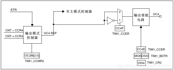
TIM1的OC模块,可以产生PWM波形,具体步骤;
- 寄存器
TIMx CNT每过一个时钟周期就会加1; - 然后
TIMx CNT的值与TIMx CCER进行比较; - 最终改变
OC上的有效电平;
以上只需要配置好TIM1的寄存器即可,无需再编程干预,当然可以动态修改TIMx CCER的值,从而改变占空比。可以参考下图;
PWM模式
这里主要对PWM模式进行配置的时候做一下区分,存在以下两种情况;
TIM_OCInitStructure.TIM_OCMode = TIM_OCMode_PWM1;TIM_OCInitStructure.TIM_OCMode = TIM_OCMode_PWM2;
那么TIM_OCMode_PWM1和TIM_OCMode_PWM2有什么区别呢?
- TIM_OCMode_PWM1 PWM模式1
在向上计数时,一旦TIMx_CNT<TIMx_CCR1时通道1为有效电平,否则为无效电平
在向下计数时,一旦TIMx_CNT>TIMx_CCR1时通道1为无效电平(OC1REF=0),否则为有效 电平(OC1REF=1)。 - TIM_OCMode_PWM2 PWM模式2
在向上计数时,一旦TIMx_CNT<TIMx_CCR1时通道1为无效电平,否则为有效电平
在向下计数时,一旦TIMx_CNT>TIMx_CCR1时通道1为有效电平,否则为无效电平。
死区插入和刹车功能
互补PWM还支持插入死区时间,最主要的寄存器是TIMx_BDTR,在标准库中把相关的变量封装到TIM_BDTRInitTypeDef结构体中;具体如下;
typedef struct
{

  uint16_t TIM_OSSRState;        /*!< Specifies the Off-State selection used in Run mode.
                                      This parameter can be a value of @ref OSSR_Off_State_Selection_for_Run_mode_state */

  uint16_t TIM_OSSIState;        /*!< Specifies the Off-State used in Idle state.
                                      This parameter can be a value of @ref OSSI_Off_State_Selection_for_Idle_mode_state */

  uint16_t TIM_LOCKLevel;        /*!< Specifies the LOCK level parameters.
                                      This parameter can be a value of @ref Lock_level */

  uint16_t TIM_DeadTime;         /*!< Specifies the delay time between the switching-off and the
                                      switching-on of the outputs.
                                      This parameter can be a number between 0x00 and 0xFF  */

  uint16_t TIM_Break;            /*!< Specifies whether the TIM Break input is enabled or not.
                                      This parameter can be a value of @ref Break_Input_enable_disable */

  uint16_t TIM_BreakPolarity;    /*!< Specifies the TIM Break Input pin polarity.
                                      This parameter can be a value of @ref Break_Polarity */

  uint16_t TIM_AutomaticOutput;  /*!< Specifies whether the TIM Automatic Output feature is enabled or not.
                                      This parameter can be a value of @ref TIM_AOE_Bit_Set_Reset */
} TIM_BDTRInitTypeDef;
相关的含义看注释可以知道大概意思;这里整理了几个比较重要的变量;
- 死区时间
TIM_DeadTime的计算;TIMx_BDTR的低八位的配置决定了死区的时间;
UTG[7:0]: 死区发生器设置 (Dead-time generator setup)
这些位定义了插入互补输出之间的死区持续时间。假设DT表示其持续时间:
| DTG[7:5]=0xx => DT=DTG[7:0] × Tdtg | Tdtg = TDTS; |
| DTG[7:5]=10x => DT=(64+DTG[5:0]) × Tdtg | Tdtg = 2 × TDTS; |
| DTG[7:5]=110 => DT=(32+DTG[4:0]) × Tdtg | Tdtg = 8 × TDTS; |
| DTG[7:5]=111 => DT=(32+DTG[4:0])× Tdtg | Tdtg = 16 × TDTS; |
例:若TDTS = 125ns(8MHZ),可能的死区时间为:
0到15875ns,若步长时间为125ns;
16us到31750ns,若步长时间为250ns;
32us到63us,若步长时间为1us;
64us到126us,若步长时间为2us;
注:一旦LOCK级别(TIMx_BDTR寄存器中的LOCK位)设为1、 2或3,则不能修改这些位。
TIM_Break则表示是否决定使用刹车,如果发生错误,则可以通过刹车,第一时间停止PWM波形的产生,从而保证了系统的安全性;
代码实现
#include "stm32f10x.h"
#include "svpwm_driver.h"
#include "stm32f10x_tim.h"
#include "stm32f10x_it.h"
#include <stdio.h>

#define SVPWM_USE_BDT 	1
#define USE_HARD_PWM 	1
/**
  * @brief  Configures the different system clocks.
  * @param  None
  * @retval None
  */
void pwm_rcc_init(void)
{
  /* TIM1, GPIOA, GPIOB, GPIOE and AFIO clocks enable */
  RCC_APB2PeriphClockCmd(RCC_APB2Periph_TIM1 | RCC_APB2Periph_GPIOA |
                         RCC_APB2Periph_AFIO |
                         RCC_APB2Periph_GPIOB, ENABLE);
}

void pwm_cnt_irq_init(void)
{

}

/**
  * @brief  Configure the TIM1 Pins.
  * @param  None
  * @retval None
  * @note
  *			PA8 /T1_CH1  ---> HIn3
  *			PA9 /T1_CH2  ---> HIn2
  *			PA10/T1_CH3  ---> HIn1
  *										Out2 ---> PA0/ADC0
  *										Out3 ---> PA1/ADC1
  *			PB15/T1_CHN3 ---> LIn1
  *			PB14/T1_CHN2 ---> LIn2
  *			PB13/T1_CHN1 ---> LIn3
  */
void pwm_pin_init(void)
{
	GPIO_InitTypeDef GPIO_InitStructure;

	/* GPIOA Configuration: Channel 1, 2 and 3 as alternate function push-pull */
	GPIO_InitStructure.GPIO_Pin = GPIO_Pin_8 | GPIO_Pin_9 | GPIO_Pin_10 ;
	GPIO_InitStructure.GPIO_Mode = GPIO_Mode_AF_PP;
	GPIO_InitStructure.GPIO_Speed = GPIO_Speed_50MHz;
	GPIO_Init(GPIOA, &GPIO_InitStructure);

	/* GPIOB Configuration: Channel 1N, 2N and 3N as alternate function push-pull */
	GPIO_InitStructure.GPIO_Pin = GPIO_Pin_13 | GPIO_Pin_14 | GPIO_Pin_15;

	GPIO_Init(GPIOB, &GPIO_InitStructure);
}

void pwm_tim_init(void){

	TIM_TimeBaseInitTypeDef  TIM_TimeBaseStructure;
	TIM_OCInitTypeDef  TIM_OCInitStructure;
	TIM_BDTRInitTypeDef      TIM_BDTRInitStructure;
//	NVIC_InitTypeDef 	NVIC_InitStructure;
	uint16_t TimerPeriod = 0;
	uint16_t Channel1Pulse = 0, Channel2Pulse = 0, Channel3Pulse = 0;

	/* TIM1 Configuration ---------------------------------------------------
	 Generate 7 PWM signals with 4 different duty cycles:
	 TIM1CLK = SystemCoreClock, Prescaler = 0, TIM1 counter clock = SystemCoreClock
	 SystemCoreClock is set to 72 MHz for Low-density, Medium-density, High-density
	 and Connectivity line devices and to 24 MHz for Low-Density Value line and
	 Medium-Density Value line devices

	 The objective is to generate 7 PWM signal at 17.57 KHz:
	   - TIM1_Period = (SystemCoreClock / 17570) - 1
	 The channel 1 and channel 1N duty cycle is set to 50%
	 The channel 2 and channel 2N duty cycle is set to 50%
	 The channel 3 and channel 3N duty cycle is set to 50%
	 The Timer pulse is calculated as follows:
	   - ChannelxPulse = DutyCycle * (TIM1_Period - 1) / 100
	----------------------------------------------------------------------- */
	TimerPeriod = (SYS_FRQ / PWM_FRQ ) - 1;
	/* Compute CCR1 value to generate a duty cycle at 50% for channel 1 and 1N */
	Channel1Pulse = (uint16_t) (((uint32_t) PWM_DUTY * (TimerPeriod - 1)) / 100);
	/* Compute CCR2 value to generate a duty cycle at 37.5%  for channel 2 and 2N */
	Channel2Pulse = (uint16_t) (((uint32_t) PWM_DUTY * (TimerPeriod - 1)) / 100);
	/* Compute CCR3 value to generate a duty cycle at 25%  for channel 3 and 3N */
	Channel3Pulse = (uint16_t) (((uint32_t) PWM_DUTY * (TimerPeriod - 1)) / 100);

	//TIM_DeInit(TIM1);

	/* Time Base configuration */
	TIM_TimeBaseStructure.TIM_Prescaler = TIM_PSCReloadMode_Update;
	//TIM_TimeBaseStructure.TIM_CounterMode = TIM_CounterMode_Up;//
	TIM_TimeBaseStructure.TIM_CounterMode = TIM_CounterMode_CenterAligned2;
	TIM_TimeBaseStructure.TIM_Period = TimerPeriod;
	TIM_TimeBaseStructure.TIM_ClockDivision = TIM_CKD_DIV1;
	TIM_TimeBaseStructure.TIM_RepetitionCounter = 0;

	TIM_TimeBaseInit(TIM1, &TIM_TimeBaseStructure);
	/*
	TIM_ClearFlag(TIM1, TIM_FLAG_Update);
	TIM_ITConfig(TIM1,TIM_IT_Update, ENABLE);
	NVIC_InitStructure.NVIC_IRQChannel = TIM1_UP_IRQn;
	NVIC_InitStructure.NVIC_IRQChannelPreemptionPriority = 0x00;
	NVIC_InitStructure.NVIC_IRQChannelSubPriority = 0x02;
	NVIC_InitStructure.NVIC_IRQChannelCmd = ENABLE;
	NVIC_Init(&NVIC_InitStructure);
	*/
	/* Channel 1, 2, 3 Configuration in PWM mode */
	#if USE_HARD_PWM

	/**
	TIM_OCMode_PWM1	PWM模式1
	在向上计数时,一旦TIMx_CNT<TIMx_CCR1时通道1为有效电平,否则为无效电平
	在向下计数时,一旦TIMx_CNT>TIMx_CCR1时通道1为无效电平(OC1REF=0),否则为有效 电平(OC1REF=1)。
	TIM_OCMode_PWM2 PWM模式2
	在向上计数时,一旦TIMx_CNT<TIMx_CCR1时通道1为无效电平,否则为有效电平
	在向下计数时,一旦TIMx_CNT>TIMx_CCR1时通道1为有效电平,否则为无效电平。
	*/
	TIM_OCInitStructure.TIM_OCMode = TIM_OCMode_PWM1;
	TIM_OCInitStructure.TIM_OutputState = TIM_OutputState_Enable;
	TIM_OCInitStructure.TIM_OutputNState = TIM_OutputNState_Enable;
	TIM_OCInitStructure.TIM_Pulse = Channel1Pulse;
	TIM_OCInitStructure.TIM_OCPolarity = TIM_OCPolarity_High;
	TIM_OCInitStructure.TIM_OCNPolarity = TIM_OCPolarity_High;
	TIM_OCInitStructure.TIM_OCIdleState = TIM_OCIdleState_Reset;
	TIM_OCInitStructure.TIM_OCNIdleState = TIM_OCIdleState_Reset;

	TIM_OC1Init(TIM1, &TIM_OCInitStructure);

	TIM_OCInitStructure.TIM_Pulse = Channel2Pulse;
	TIM_OC2Init(TIM1, &TIM_OCInitStructure);

	TIM_OCInitStructure.TIM_Pulse = Channel3Pulse;
	TIM_OC3Init(TIM1, &TIM_OCInitStructure);

	TIM_OC1PreloadConfig(TIM1,TIM_OCPreload_Enable);
	TIM_OC2PreloadConfig(TIM1,TIM_OCPreload_Enable);
	TIM_OC3PreloadConfig(TIM1,TIM_OCPreload_Enable);

	#endif

#if SVPWM_USE_BDT
	TIM_BDTRInitStructure.TIM_OSSRState = TIM_OSSRState_Enable;
	TIM_BDTRInitStructure.TIM_OSSIState = TIM_OSSIState_Enable;
	TIM_BDTRInitStructure.TIM_LOCKLevel = TIM_LOCKLevel_OFF;
	TIM_BDTRInitStructure.TIM_DeadTime = 30;
	TIM_BDTRInitStructure.TIM_Break = TIM_Break_Disable;
	TIM_BDTRInitStructure.TIM_BreakPolarity = TIM_BreakPolarity_Low;
	TIM_BDTRInitStructure.TIM_AutomaticOutput = TIM_AutomaticOutput_Disable;
	TIM_BDTRConfig(TIM1, &TIM_BDTRInitStructure);
#endif
	TIM_CCPreloadControl(TIM1,ENABLE);
	/* TIM1 counter enable */
	TIM_Cmd(TIM1, ENABLE);
	/* TIM1 Main Output Enable */
	TIM_CtrlPWMOutputs(TIM1, ENABLE);
}

void pwm_init(void){
	pwm_rcc_init();
	pwm_pin_init();
	pwm_cnt_irq_init();
	pwm_tim_init();
}

int32_t get_pwm_period(void){
	return (int32_t)((SYS_FRQ / PWM_FRQ ) - 1);
}

void pwm_reset_duty_cnt(uint8_t index, int16_t cnt){
	if(cnt <= 0){
		cnt = get_pwm_period()/2;
	}
	switch(index){
		case 1:
			TIM1->CCR1 = (uint16_t)cnt;
		break;
		case 2:
			TIM1->CCR2 = (uint16_t)cnt;
		break;
		case 3:
			TIM1->CCR3 = (uint16_t)cnt;
		break;
	}
}

void pwm_disable(void){
	TIM_CtrlPWMOutputs(TIM1, DISABLE);
}

void pwm_enable(void){
	TIM_CtrlPWMOutputs(TIM1, ENABLE);
}
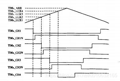
以上代码主要实现以下几个功能;
- IM1定时器时钟,使用中央对齐模式1,则会产生上溢信号;
- PWM模式设置为
TIM_OCMode_PWM1; - 加入了死区;
- 占空比 50%;
具体如下图所示;
参考
http://www.stmcu.org.cn/module/forum/thread-613602-1-1.html