By Achronix
Intelligent server adapters, or SmartNICs, boost server performance in cloud and private data centers by offloading network processing workloads and tasks from server CPUs. Offloading network processing to a SmartNIC is not a new concept — for example, there are NICs that offload some network-processing functions such as checksum computation and segmentation. However, the rapid explosion in data-center network traffic driven by software-defined networking (SDN), Open vSwitch (OVS), and network functions virtualization (NFV) demands a new class of NIC with even greater offload capabilities: the SmartNIC.

SmartNICs provide several significant benefits to data-center networks including:
- Accelerating network, storage, and compute tasks by executing them directly on the network interface card, eliminating the need to run these workloads on servers and freeing up CPU cycles, thus dramatically improving server performance and reducing overall power consumption resulting in lower system-level total cost of ownership.
- Offloading increasingly complex networking tasks including overlay tunneling protocols such as VxLAN and complex virtual switching from server processors, freeing the server processors to perform actual, revenue-generating tasks.
- Improving effective network bandwidth and throughput by executing offloaded functions in fast hardware instead of slower software.
- Providing additional, flexible functionality that easily accommodates new and constantly changing networking and storage protocols.
A successful SmartNIC design must be able to implement complex data-plane functions including multiple matchaction processing, tunnel termination and origination, traffic metering, and traffic shaping. A SmartNIC should also provide the host processor with per-flow statistics to inform network-tuning algorithms. In addition, the SmartNIC's high-speed data plane should be programmable through either downloadable updates or network programming to enable a flexible architecture that can easily adapt to changing data plane requirements. A successful SmartNIC design must work seamlessly with existing data-center ecosystems. Otherwise, the SmartNIC design is unlikely to succeed.
The Three Forms of SmartNICs
SmartNIC designs currently take one of three forms:
- Multicore SmartNICs, based on ASICs containing multiple CPU cores
- FPGA-based SmartNICs
- FPGA-augmented SmartNICs, which combine hardware-programmable FPGAs with ASIC network controllers
A multicore SmartNIC design likely includes an ASIC that incorporates many software-programmable microprocessor cores. These cores are typically higher performance Arm processors, which process packets and offload from the main (and expensive) server CPUs. Multicore SmartNIC ASICs may also incorporate fixedfunction hardware engines that can offload well-defined tasks such as standardized security and storage protocols.
However, multicore SmartNICs suffer from at least two limitations:
- They are based on software-programmable processors which are slower when used for network processing due to a lack of processor parallelism.
- The fixed-function hardware engines in these multicore ASICs lack the data-plane programmability and flexibility that is increasingly required for SmartNIC offloading.
Processor-based, multicore SmartNIC designs became more widely available with the 10G NIC generation. However, these software-centric, multicore SmartNICs have been hard-pressed to keep pace as Ethernet data rates in data centers have risen from 10G to 25G, 40G, 50G, 100G, and beyond. These multicore SmartNICs simply cannot achieve the required peak bandwidths at these higher data rates. Meanwhile, the fixed-function engines in a multicore SmartNIC ASIC cannot be stretched to handle new encryption or security algorithms because they lack sufficient programmability to accommodate anything more than slight algorithmic changes.
FPGA-Based SmartNICs
An FPGA-based SmartNIC employs the expanded hardware programmability of FPGAs to build any data-plane functions required by the tasks offloaded to the SmartNIC. Because FPGAs are reprogrammable, the data-plane functions implemented by the FPGA can be torn down and reconfigured at will and in real time. All such offloaded functions operate at hardware – not software – speeds.
FPGA-based SmartNIC designs can accelerate network functions by several orders of magnitude over implementations based purely on software. Use of FPGAs in SmartNIC designs delivers the wire-speed performance and power efficiency of custom hardware with the ability to create deep packet/network processing pipelines that support complex offload tasks and improve single-flow network performance. Replicating these pipelines by exploiting the large amount of hardware parallelism inherent in FPGAs improves megaflow performance enough to meet the high-performance, high-bandwidth, high-throughput needs of next-generation data-center architectures based on speedier Ethernet networks.
The FPGA-Augmented SmartNIC
The need for backwards compatibility has given rise to another type of SmartNIC – the FPGA-augmented SmartNIC – which adds FPGA capabilities to the NIC. Based on the design, the NIC can be either an existing multicore SmartNIC or just a simple NIC ASIC. The NIC incorporated into these designs provides backward compatibility, particularly with hypervisors. Consequently, an FPGA-augmented SmartNIC design based on an existing NIC, with an FPGA added for capability expansion, can be monetized immediately because it is automatically compatible with existing networking APIs and interface protocols and can, therefore, use existing APIs and drivers. The on-board FPGA in a FPGA-augmented SmartNIC design enables significantly higher performance and feature expansion.
There are three ways to develop an FPGA-augmented SmartNIC design. The first is to simply connect an FPGA to an existing NIC. An alternative is to design a next-generation SmartNIC ASIC that incorporates an FPGA array on the chip. A third alternative involves adding a high-speed, chip-to-chip interconnect to the SmartNIC ASIC’s design and develop an FPGA chiplet to connect to the SmartNIC ASIC. All three design approaches have advantages and disadvantages.
Basing an FPGA-augmented SmartNIC design on an existing NIC has the advantage of guaranteed compatibility. Existing drivers, APIs, and interface protocols will be unchanged for existing functions because they are implemented on the existing NIC. Extensions to the existing APIs and drivers are only needed for functional extensions implemented in the attached FPGA.
The disadvantages of this approach are somewhat structural. First, if the existing design lacks any sort of interface for an expansion chip, including an FPGA, then the FPGA will need to connect directly to the host interface bus and the Ethernet ports in parallel with the NIC. If the design does have an interface for an external accelerator, that interface may possibly present a bandwidth bottleneck to the massive amount of Ethernet packet traffic that the FPGA must handle.
For maximum performance, both the NIC components and the FPGA should reside on the same piece of silicon. This approach requires an embedded FPGA (eFPGA). Incorporating an eFPGA into a NIC maximizes the usable bandwidth between the FPGA functionality and the rest of the NIC that results in faster transfer rates from the direct, on-die connections to the eFPGA.
An intermediate design approach involves a respin of the SmartNIC ASIC. In this, a high-speed die-to-die interface is added to connect the ASIC to an FPGA chiplet. The combined solution is then combined in an multichip module (MCM). The advantage to this approach is that only a minimal change to the SmartNIC ASIC is needed, which lowers the design risk. This chiplet-based design approach also introduces the possibility of a delete option for the SmartNIC’s design, which can be offered in chip or board form with and without the FPGA at different price points. The disadvantage to this approach is that the chip-to-chip interconnect within the MCM will possibly provide less bandwidth than an on-die interconnect.
Building a SmartNIC, Step By Step
SmartNICs are used in different deployments including storage, security, and network processing. As shown in the figure below, the eventual goal is have solution that consumes fewer processors cores and, at the same time, offers higher performance at a reduced cost.
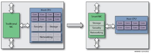
Figure 1: A SmartNIC Frees up Processor Cores
The definitions for a SmartNIC are expansive and include a large hierarchy of capabilities, all built on a basic NIC foundation. Example 1 through 13 illustrate the many processing elements that can be added to a NIC to create increasingly more powerful SmartNICs. These features can easily be added or deleted as needed when the SmartNIC is implemented with some form of FPGA. An FPGA-based and FPGA-augmented SmartNIC implementation also permits easy, remote modification or improvement to each task-acceleration feature and can be made even after the SmartNIC has been installed in a data-center server.
Example 1 shows an example of the basic NIC foundation, employing multiple Ethernet MACs and a PCIe block for the host-processor interface. A host processor must then handle all of the Ethernet traffic.
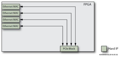
Figure 2: Example 1 – Basic NIC Foundation
Example 2 adds a DMA engine to a basic NIC reduces the host processor's workload by allowing the NIC to move Ethernet traffic between the Ethernet MACs and server memory without significant server CPU intervention.
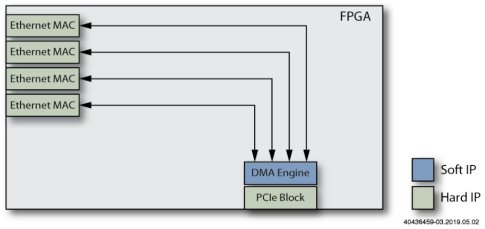
Figure 3: Example 2 – Adding a DMA Engine to a Basic NIC
Example 3 adds a filtering engine that further reduces the host processor's task load by blocking packets that do not require the processor's attention.
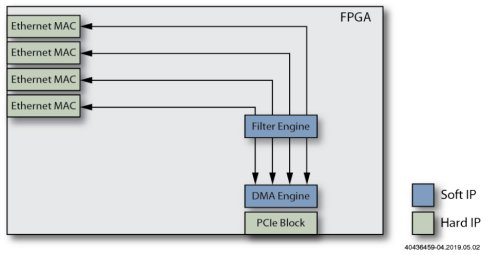
Figure 4: Example 3 – Adding a Filtering Engine
Example 4 adds external DRAM to the filtering engine which significantly increases the number of rules that the SmartNIC can use for filtering. With enough external memory, the SmartNIC can manage millions of rules.
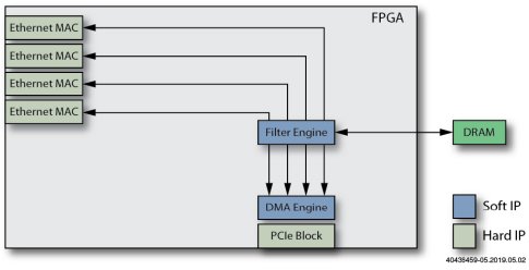
Figure 5: Example 4 – Adding External DRAM to the Filtering Engine
Example 5 adds an L2/L3 offload engine that can further reduce the host CPU workload by handling lower-layer switching and routing among the SmartNIC's Ethernet ports. To be effective, the L2/L3 offload engine will require a large external DRAM to buffer network packets.
Note
The interface between the SmartNIC FPGA or ASIC and the external DRAM must meet the bandwidth requirement of the Ethernet traffic being switched.
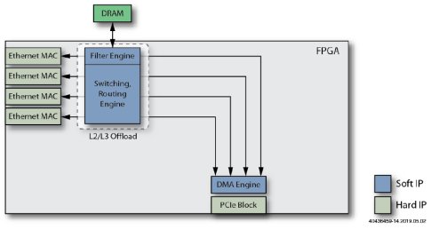
Figure 6: Example 5 – Adding an L2/L3 Offload Engine
Example 6 adds a tunneling engine to allow the SmartNIC to offload various tunnel encapsulations and further relieve the processor of cycle-intensive tunneling requirements.
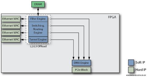
Figure 7: Example 6 – Adding a Tunneling Engine
Example 7 adds fast external memory to allow the SmartNIC to deeply buffer incoming network packets, enabling wire-speed packet switching and hierarchical QoS scheduling with multiple queues.
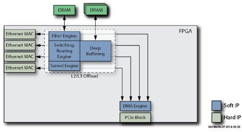
Figure 8: Example 7 – Adding Deep Packet Buffers
Example 8 adds a flow engine with its own DRAM buffer to enable the SmartNIC's routing engine to handle millions of routing-table entries. The flow engine helps to offload network address translation/protocol address translation (NAT/PAT) operations.
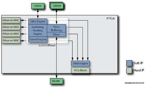
Figure 9: Example 8 – A SmartNIC with Flow Engine
Example 9 adds a TCP offload engine to handle full/part of the TCP stack which increases SmartNIC performance without consuming more CPU cycles.
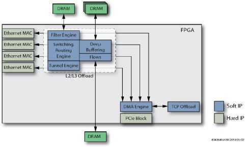
Figure 10: Example 9 – A TCP Offload Engine
Example 10 adds a partial/full security engine to the SmartNIC offloads encryption and decryption tasks from the host CPU on a per-flow basis.
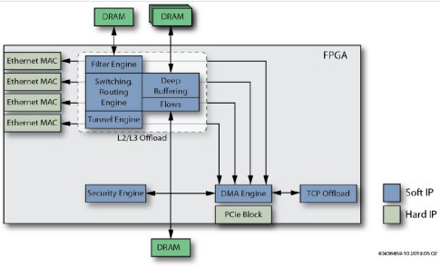
Figure 11: Example 10 – Adding a Security Engine to Offload Encryption and Decryption Tasks
Example 11 adds a separate QoS engine to allow the SmartNIC to manage service-level agreements (SLAs) without intervention from the server CPU.
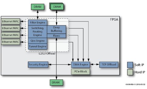
Figure 12: Example 11 – Adding a Separate QoS Engine to Manage SLAs
Example 12 adds a programmable packet decoder that incorporates P4-like programmability into the SmartNIC. P4 is a standard network programming language specifically designed to describe and program the operation of packet-forwarding planes.
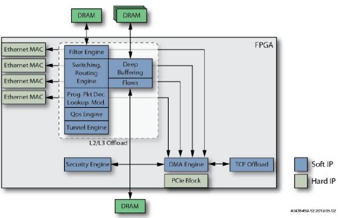
Figure 13: Example 12 – The Addition of a Programmable Packet Decoder
Example 13 adds one or more on-board processors that provides the SmartNIC with full software programmability (for tasks such as OAM, etc.), further enabling the offloading of server CPUs.
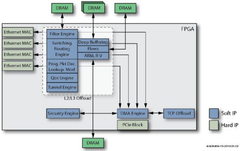
Figure 14: Example 13 – SmartNIC with On-board Processors
One of the biggest obstacles to adopting SmartNIC designed with FPGA in data centers is the engineering inertia caused by the huge success that software-based multicore SmartNICs enjoyed in the 10G era. Networking offload and acceleration techniques have adopted and standardized on APIs and interface protocols that permit server tasks to interact with certain multicore SmartNICs. Every server software stack targets a few specific NICs and SmartNICs. The APIs and drivers that have been developed for existing NICs and SmartNICs are hardcoded into these software stacks that run on server CPUs. Unless a SmartNIC designed with an FPGA supports these existing APIs and emulates the existing interface protocols, putting these SmartNICs into service requires modifications to the software stacks.
Achronix's Technology Offerings for SmartNIC Design
Achronix provides a range o FPGA technologies for all of these FPGA-enhanced SmartNIC architectures. These alternatives include Speedster®7t FPGAs, Speedchip™ FPGA chiplets, and Speedcore™ eFPGA IP. Built on TSMC’s 7nm FinFET process technology, Speedster7t FPGAs feature a revolutionary and new 2D network-on-chip (NoC), 4 Tbps GDDR6 memory interfaces, 400G Ethernet controllers and PCI Express Gen5 ports optimized for enhanced SmartNIC architectures. In this example, an Achronix Speedster7t FPGA can be used to leverage an existing NIC chip in either one of two ways, as a bump-in-the-wire accelerator or as a sidecar accelerator, as shown below.
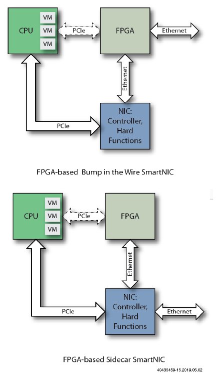
Figure 15: SmartNIC Architectures Using FPGAs Include "Bump-in-the-Wire" and Sidecar Designs
For the bump-in-the-wire architecture, all network data flows through the FPGA from the external Ethernet connections. The FPGA handles the acceleration tasks and passes packets to the NIC device for additional processing. This design approach provides superior acceleration of intensive data-path functions, such as cryptography or compression, and full flexibility for exception handling.
For the sidecar architecture, all data from the external Ethernet connection flows through the NIC device. Any data that requires additional processing is then passed to the FPGA either directly over the Ethernet ports or through the server CPU, typically over a fast PCIe connection. The sidecar architecture is generally less flexible than the bump-in-the-wire approach.
Note
The FPGA used for these two architectures can be a standalone FPGA such as the Achronix's Speedster7t FPGA, or a Speedcore eFPGA with customized programmable-hardware resources for specialized network-processing requirements embedded within a SoC.
Using a standard FPGA to implement this form of SmartNIC offers the fastest time to market because the FPGA is an off-the-shelf device. However, for increased performance, lower power and smaller form factors, the FPGA functions can be integrated into a custom SoC which incorporates CPU, peripherals plus Speedcore eFPGA fabric tailored specifically to the application requirements.
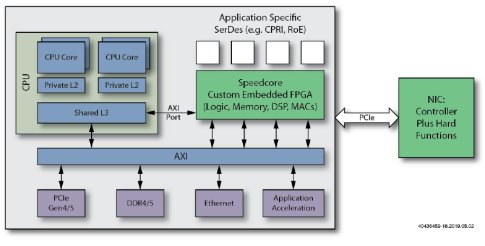
Figure 16: A SmartNIC Incorporating a Speedcore eFPGA to Reduced Cost, Power and Footprint
The next option in FPGA-accelerated SmartNIC employs a Speedchip FPGA chiplet on an MCM rather than a packaged FPGA. This design approach allows the use of a high-speed, chip-to-chip, ultrashort short range (USR) SerDes interconnect between the NIC chip and the FPGA chiplet. A SmartNIC that incorporates a Speedchip FPGA chiplet delivers all of the advantages of an FPGA-augmented SmartNIC plus the additional performance that results from the higher-speed interconnect between the FPGA chiplet and the NIC ASIC, but without the additional cost of a full system redesign since the same base chip and its interfaces are reused.
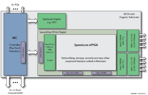
Figure 17: Speedchip FPGA Chiplet Powered SmartNIC
The Speedchip chiplet used in this design is a custom device, so the amount and distribution of on-chip resources and on-chip interconnect within the FPGA can be optimized for the target SmartNIC application(s). A fast PCIe port or a suitable USR SerDes can provide the die-to-die interconnect performance that meets the application's bandwidth requirements.
As with the architecture based on packaged FPGAs, this chiplet-based design can employ either the bump-in-thewire or the sidecar configuration. Naturally, this approach requires that the NIC ASIC incorporate an appropriate PCIe or USR SerDes to communicate with the FPGA chiplet.
An all-in-one, SmartNIC ASIC based on Achronix's Speedcore eFPGA, shown below, maximizes the SmartNIC's performance, programmability, and flexibility. Achronix is the only FPGA vendor that can enable both standalone and integrated SmartNIC architectures which simplifies supplier engagement models and provides one solution provider which can easily scale to provide the optimal solution.
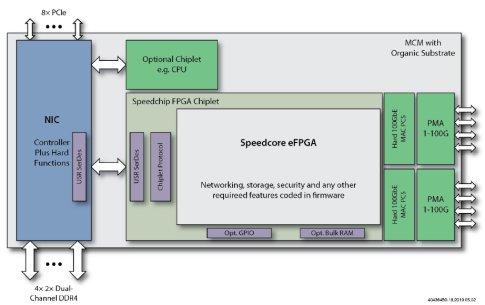
Figure 18: A SmartNIC Incorporating a Speedcore eFPGA Maximizes Performance, Programmability, and Flexibility
As with the chiplet-based approach, the Speedcore eFPGA can be tailored and optimized to meet the SmartNIC's exact requirements. In addition, as an IP core in the NIC ASIC, the Speedcore eFPGA can be equipped with nearly any amount of I/O bandwidth required by the application. The eFPGA's connections to the rest of the logic on the NIC ASIC can include hundreds or thousands of parallel interconnect lines, PCIe connections, or many other sorts of high-speed serial protocols.
Achronix's ACE design tools provide the FPGA design and configuration capabilities required by all of these FPGA alternatives, which means that the same FPGA designs can be deployed, starting with a packaged Speedster7t FPGA design and then evolving to a chiplet-based or eFPGA design to either boost performance or reduce manufacturing costs in high-volume applications. Achronix's unique ability to support packaged Speedster FPGAs, Speedchip FPGA chiplets, and Speedcore eFPGAs with one common tool set represents a significant design advantage for SmartNIC developers.
Conclusion
The exponential rise in network traffic in data centers increasingly burdens host server CPUs, which spend more of their time managing networking flows instead of running applications. These network-management tasks consume CPU cycles while increasing the cost for data-center operators. SmartNICs can offload a lot of these network-management tasks from the host CPUs thereby freeing up the processor cycles that can then be monetized resulting in lower total cost of ownership of the servers.
While it is possible to implement SmartNICs without FPGAs, incorporating an FPGA into a SmartNIC's design significantly enhances its data-plane flexibility and programmability — the data plane is where the SmartNIC's most work-intensive networking tasks reside. FPGA-based and FPGA-augmented SmartNICs excel at handling these complex, high-speed tasks, whether the FPGA is realized as a packaged device, as an FPGA chiplet in a SmartNIC MCM, or as a programmable FPGA IP core in a SmartNIC ASIC.
Achronix is the only vendor which provides FPGAs in all three of these forms and supports these solutions using a common design flow within Achronix's ACE development tools. Achronix makes it possible to start a SmartNIC design using an off-the-shelf, packaged Speedster7t FPGA device providing the fastest time to market. As production volumes increase and additional cost and power reduction is needed, designers can switch to a chiplet-based MCM. Finally for the ultimate in cost and power reduction, designers can create a custom ASIC design leveraging eFPGA technology using the same design environment and without having to switch to a new vendor. Achronix's Speedster7t FPGAs, Speedchip FPGA chiplets and Speedcore eFPGA IP technology provide a unique combination of data interfacing, storage, movement and processing capabilities making it ideal for accelerating SmartNIC devices.