一、 实验要求
设计并实现一个多周期MIPS CPU,并满足如下要求:
1)仅允许使用一个存储器
2)实现六条指令:addi、add、lw、sw、bgtz、j
3)对给予的斐波那契数列例程进行测试
二、 实验原理
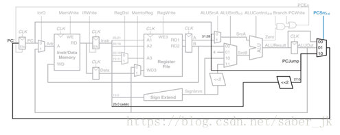
1)数据通路:

上图中不包含j指令的数据通路,添加后如下:
2)有限状态机(FSM)——状态图

三、 实验内容
1.生成IP核
为了使编码简单,这里的ram采用的是异步读,同步写,宽度32bit,深度为64.

2.主要代码分析
module top(

input clk,

input reset,

output [31:0] pc_in,

output [31:0] pc_out,

output pc_write

    );


wire [2:0]alu_op;

wire [1:0]pc_src;

wire alu_src_a;

wire [1:0]alu_src_b;

wire mem_toreg;

wire reg_write;

wire reg_dst;

wire [4:0]rd;

wire [31:0]data_out;

wire [31:0]data_out1;

wire [31:0]data_out2;

wire [31:0]data_out_a;

wire [31:0]data_out_b;

wire [31:0]data_out_out;

wire [31:0]alu_out;

wire [31:0]alu_out_out;

wire [31:0]data_write;

wire [31:0]src_a;

wire [31:0]src_b;

wire [31:0]imm;

wire mem_write;

wire ir_write;

wire [31:0]inst;

wire [31:0]addr;

wire branch_2;

wire pc_write_2;


branchand band(branch,data_out_a,branch_2);


branchor bor(branch_2,pc_write,pc_write_2);


pc pc(clk, pc_in, pc_write_2, reset, pc_out);


dataselect_32_bitaddrmux(pc_out,alu_out_out,i_or_d,addr);


ram ram(addr,data_out2,clk,mem_write,data_out);


ir ins(data_out,clk,ir_write,inst);


dataselect_5_bitregdst(inst[20:16],inst[15:11],reg_dst,rd);


data d(data_out, clk,data_out_out);


dataselect_32_bitdatamux(alu_out,data_out_out,mem_toreg,data_write);


regfilere(inst[25:21],inst[20:16],data_write,rd,reg_write,clk,data_out1, data_out2);


ab ab(data_out1,data_out2,clk,data_out_a,data_out_b);


dataselect_32_bitA(pc_out,data_out_a,alu_src_a,src_a);


signextension im(inst[15:0],imm);


dataselect_32_bit_4dataB(data_out_b,32'b1,imm,imm,alu_src_b,src_b);


alu a(src_a,src_b,alu_op,alu_out);


data aluout(alu_out,clk,alu_out_out);


dataselect_32_bit_3data pcsrc(alu_out,alu_out_out,inst[25:0],pc_src, pc_in);


controlunitcon(inst[31:26],reset,5'b0,clk,pc_write,branch,pc_src,alu_op,alu_src_a,alu_src_b,reg_write,i_or_d,ir_write,mem_write,mem_toreg,reg_dst);


endmodule
********************************************************************************************
modulecontrolunit(    //控制模块,用于译码产生控制信号,包含两个子模块

  input [5:0] opcode,

  input reset,

  input [5:0] funct,    //本实验只考虑add所以暂时用不到这个字段

  input clk,

  output pc_write,

  output branch,

  output [1:0]pc_src,

  output [2:0] alu_op,

  output alu_src_a,

  output [1:0] alu_src_b,

  output reg_write,

  output i_or_d,

  output ir_write,

  output mem_write,

  output mem_toreg,

  output reg_dst

   );


reg[3:0]now_state = 4'b0;      //当前状态

wire[3:0]next_state;                   //下一个状态


always@(posedgeclk)

       if(~reset)begin  now_state = 5'b0; end

       else

       begin

              now_state = next_state;             //根据子模块1的运算结果进行状态转换

       end


nextstatenext(now_state,opcode,next_state);//子模块1,用于运算下一个状态

control_outputout(                                   //子模块2,用于根据当前状态进行输出

                                          opcode,

                                          now_state,

                                          pc_write,

                                 branch,

                                          pc_src,

                                          alu_op,

                                 alu_src_a,

                                 alu_src_b,

                                 reg_write,

                                          i_or_d,

                                          ir_write,

                                          mem_write,

                                          mem_toreg,

                                          reg_dst);

endmodule
********************************************************************************************
module nextstate(i_state,opcode, next_state);

   input [3:0]i_state;

   input [5:0]opcode;

   output reg[3:0]next_state;


   parameter [3:0] s0 = 4'd0,

                             s1 = 4'd1,

                                            s2 = 4'd2,

                                            s3 = 4'd3,

                                            s4 = 4'd4,

                                            s5 = 4'd5,

                                            s6 = 4'd6,

                                            s7 = 4'd7,

                                            s8 = 4'd8,

                                            s9 = 4'd9,

                                            s10 = 4'd10,

                                            s11 = 4'd11;


   always @(*)


              begin

       case (i_state)


           s0: next_state = s1;

           s1:

                                   begin

                case (opcode)

                    6'b000000: next_state=  s6;           //add

                                            6'b001000: next_state =  s9;    //addi

                                            6'b100011: next_state =  s2;   //lw

                                            6'b101011: next_state =  s2;    //sw

                                            6'b000010: next_state =  s11; //jump

                                            6'b000111: next_state =  s8;  //bgtz

                endcase

                                   end


           s2:

                                   begin

                case (opcode)

                                            6'b100011: next_state =  s3;        //lw

                                            6'b101011: next_state =  s5;     //sw

                endcase

                                   end

           s3: next_state = s4;

           s4: next_state = s0;

           s5: next_state = s0;

           s6: next_state = s7;

           s7: next_state = s0;

                            s8:next_state = s0;

                            s9:next_state = s10;

                            s10:next_state = s0;

                            s11:next_state = s0;

       endcase

    end

endmodule
********************************************************************************************
module control_output(                           //根据当前state进行输出

  input[5:0] opcode,

  input[3:0] state,


 output reg pc_write,

 output reg branch,

 output reg [1:0]pc_src,

 output reg [2:0] alu_op,

 output reg alu_src_a,

 output reg [1:0]alu_src_b,

  outputreg reg_write,

 output reg i_or_d,

 output reg ir_write,

 output reg mem_write,

 output reg mem_toreg,

 output reg reg_dst

    );


parameter [3:0] s0 = 4'd0,

                s1 = 4'd1,

                                    s2 = 4'd2,

                                    s3 = 4'd3,

                                    s4 = 4'd4,

                                    s5 = 4'd5,

                                    s6 = 4'd6,

                                    s7 = 4'd7,

                                    s8 = 4'd8,

                                    s9 = 4'd9,

                                    s10 = 4'd10,

                                    s11 = 4'd11;


always @(state)

              begin

              case(state)

                     s0:

                            begin

                             pc_write=                    1;

                           branch=                      0;

                        pc_src=               2'b00;

                        alu_op=               2'b01;    //alu的操作码与ppt给定的不同

                                                                        //因为alu模块编写的不同进行了调整

                        alu_src_a=             0;

                        alu_src_b=             2'b01;

                        reg_write=                    0;

                        i_or_d=               0;

                        ir_write=              1;

                        mem_write=           0;

                        mem_toreg=           0;

                        reg_dst=              0;

                            end

                     s1:

                            begin

                             pc_write=                    0;

                        alu_src_b=            2'b11;

                        ir_write=             0;

                            end

                     s2:

                            begin

                        alu_op=            2'b01;

                        alu_src_a=            1;

                        alu_src_b=       2'b10;

                            end

                     s3:

                            begin

                        i_or_d=               1;

                            end

                     s4:

                            begin

                        reg_write=                    1;

                        mem_toreg=          1;

                        reg_dst=              0;

                            end

                     s5:

                            begin

                        i_or_d=               1;

                        mem_write=           1;

                             //pc_write =          1;

                            end

                     s6:

                            begin

                        alu_op=              2'b01;

                        alu_src_a=            1;

                        alu_src_b=            2'b00;

                            end

                     s7:

                            begin

                        reg_write=                    1;

                        mem_toreg=           0;

                        reg_dst=              1;

                            end

                     s8:

                            begin

                           branch=                      1;

                        pc_src=                 2'b01;

                        alu_op=                2'b10;

                        alu_src_a=              1;

                        alu_src_b=               2'b10;

                            end

                     s9:

                            begin

                        alu_op=               2'b01;

                        alu_src_a=            1;

                        alu_src_b=            2'b10;

                            end

                     s10:

                            begin

                        reg_write=                    1;

                        mem_toreg=           0;

                        reg_dst=               0;

                            end

                     s11:

                            begin

                             pc_write=                    1;

                        pc_src=                2'b10;

                            end

      endcase

    end

endmodule
********************************************************************************************
其余模块较为简单或者见之前实验报告,此处略去
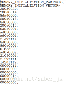
3.coe文件编写
Coe文件中存储了待运行的代码以及相关的数据,这里根据本人的设计做了响应的修改
下面是coe文件的具体内容,以及对应产生的内存数据:
4.仿真

波形图看起来比较不直观,这里主要观察指令以及状态的跳转是否正确:
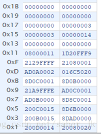
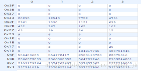
确认指令执行无误后,观察内存里的内容,如下(十进制):
四、 实验分析和总结
本实验于单周期的cpu相比,数据通路上发生了一些较为明显的变化,首先指令和数据不再分开存放,其次增加了一定数量的寄存器存储关键数据,这是由多周期指令特性决定的。
然后,多周期cpu的设计运用了有限状态机的思想,这在单周期cpu里是没有体现的,每个指令再不同的时钟周期里,其控制信号完全不同,所以需要状态机来控制状态的条状,并且根据不同指令的不同状态来决定控制信号的输出。