本次设计实验源码位于:http://download.csdn.net/detail/noticeable/9922865
实验目的:通过系统的搭建进一步了解FPGA的SOPC开发流程,并借此了姐pll IP核的应用以及用DE-SOC自带的SDRAM缓存输出数据,并为后面的工程实施提供基础。
实验现象:uart接口连接串口调试助手显示hellowold
实验步骤:
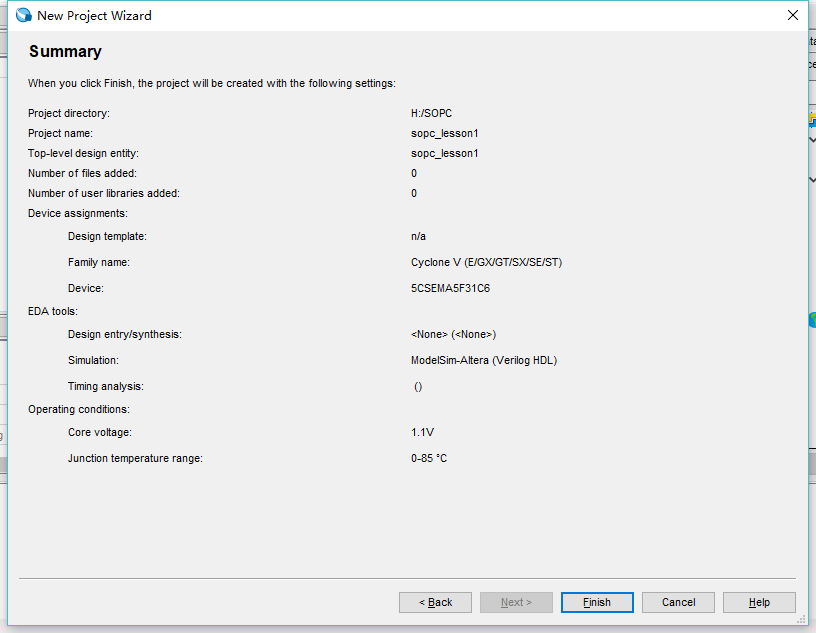
新建sopc_lesson1工程:
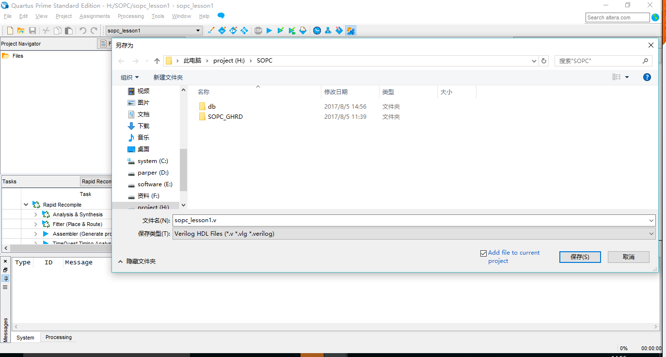
并新建一个sopc_lesson1.v文件
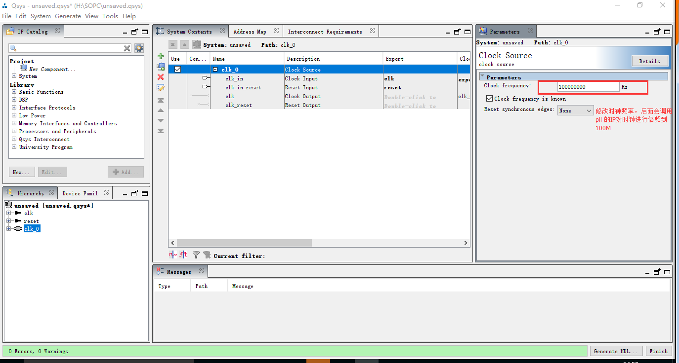
通过 打开qsys工具,修改clk_0的默认时钟
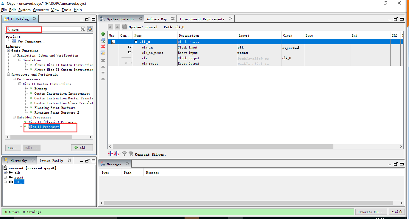
添加NIOS processor内核,且暂时不进行修改,直接finish即可。
添加存储器,由于DE-SOC开发板FPGA部分板载一块64M的SDRAM,所以这里添加SDRAM

这里的设置是按照开发板上实际的芯片参数设置的,详细操作看芯片手册,芯片手册下载地址:http://download.csdn.net/detail/noticeable/9922132
由芯片手册有
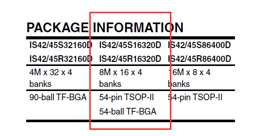
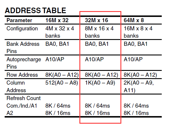

配置结果如下

timing部分的时序约束部分先不改,后面在专门运用SDRAM时再详细说明。
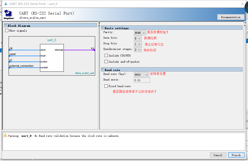
添加uart调试接口
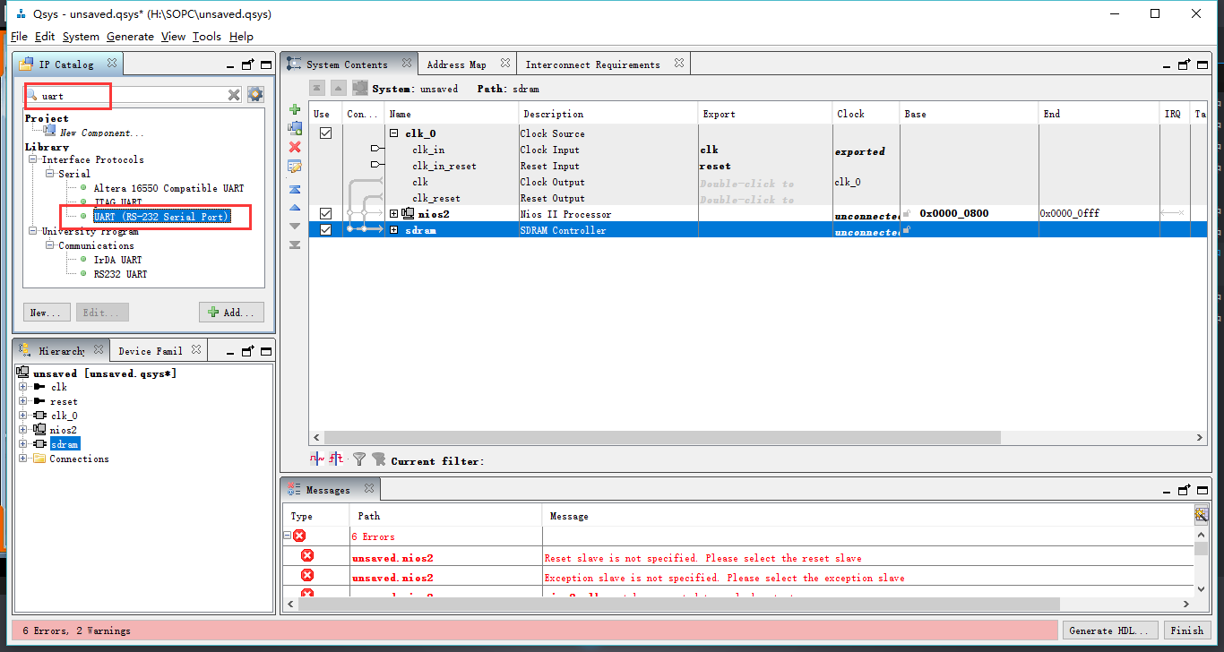
uart设置如下
基本功能设置完成后,之后即为一些与开发板相关的外设的添加:
添加pio_led的IO口
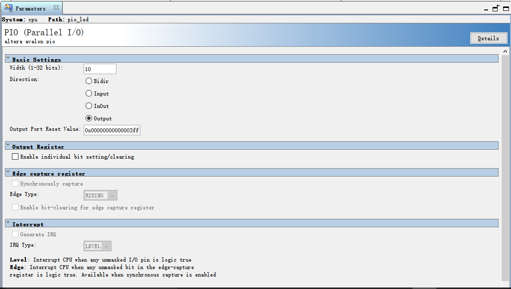
添加pio_key的IO口

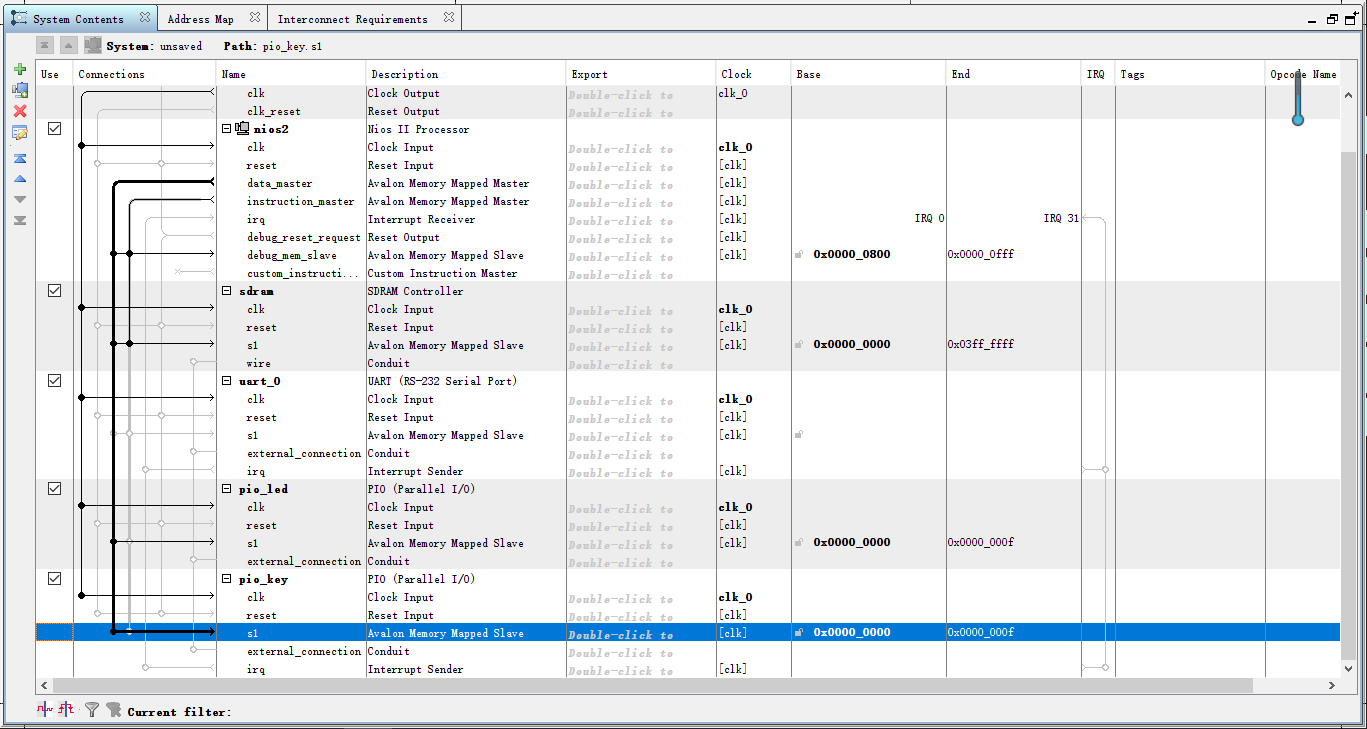
下面即是进行总线的连接
首先即是clk、控制总线和数据总线的连接
配置rst

将中断连接到CPU
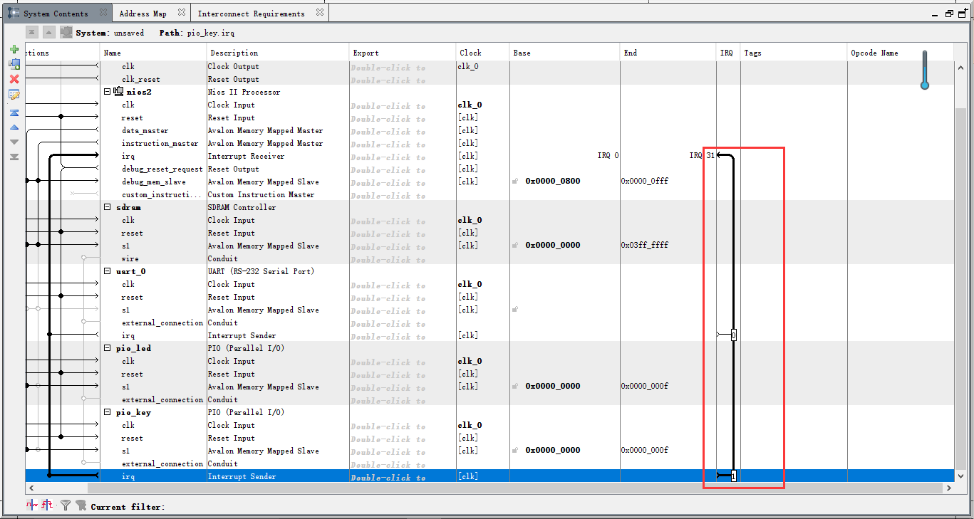
指定中断向量

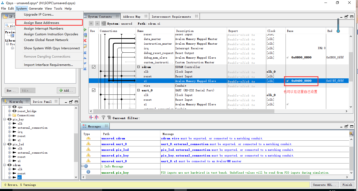
分配基地址
将引脚导出
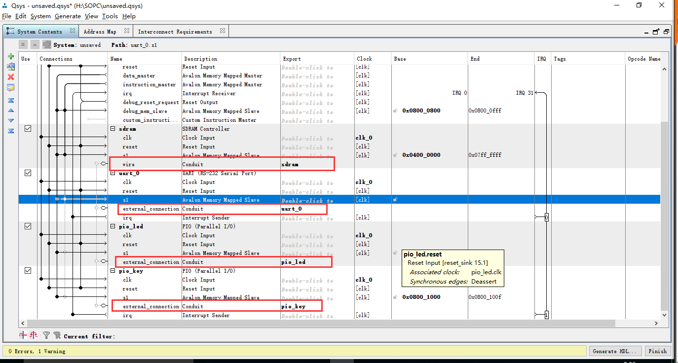
导出后发现还有一个警告,发现是uart 的s1未连接到 instruction_master上,连接上即可

连接完成后的总体连接图

将系统保存,然后点击generate->show instantiation自动生成template
然后将template复制下后,粘贴到之前生成的sopc_lesson.v文件中

最后点击generate hdl 文件
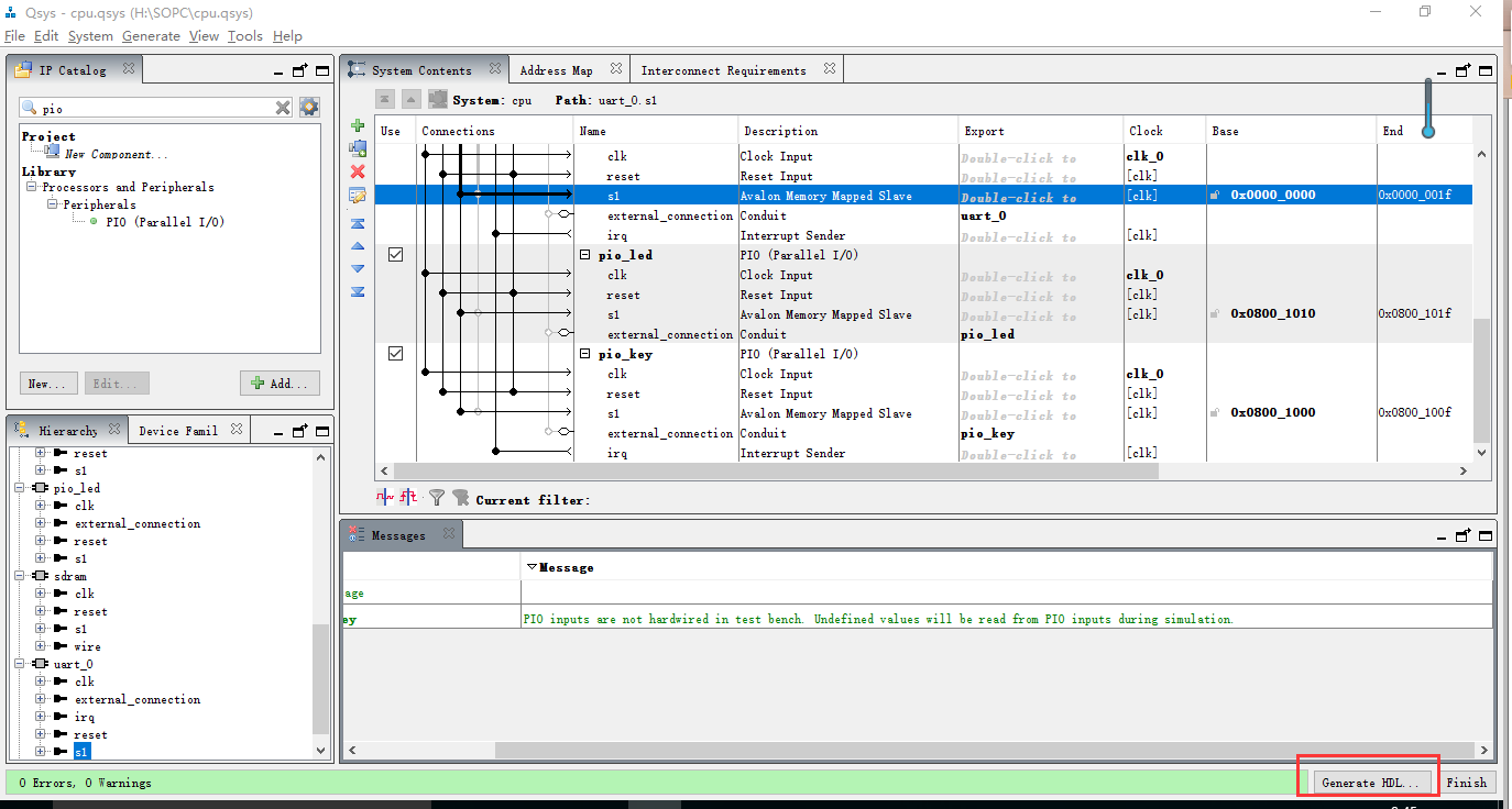
至此,设计需要的nios II软件核即设计完成了,在quartus II中将cpu.qsys文件添加到文件夹即可。
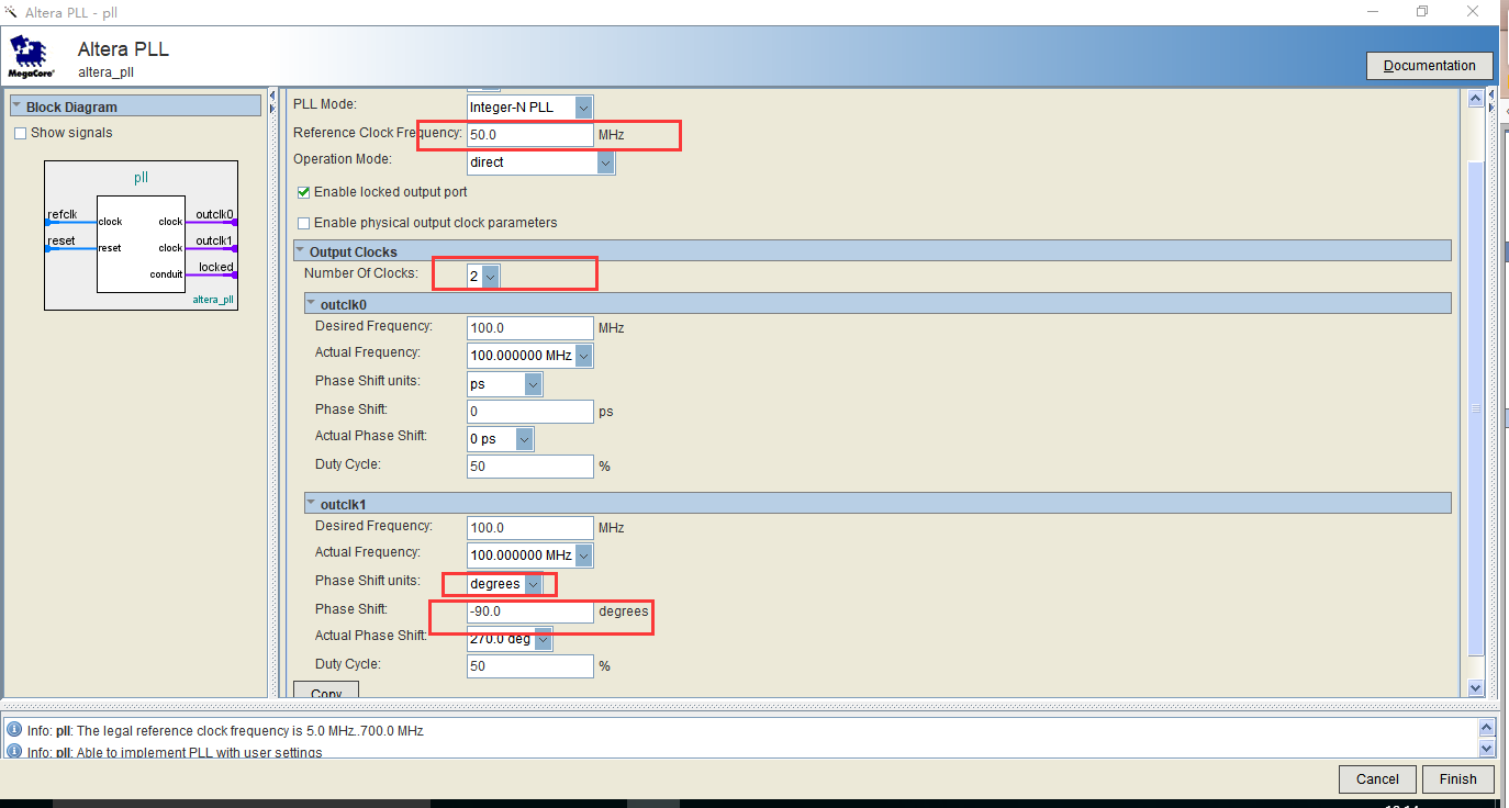
添加锁相环IP核对时钟进行倍频和移相
下面,对sopc_lesson1.v文件进行编写
module sopc_lesson1 (
        input  wire        clk_50m,        //     clk.clk
        input  wire [2:0]  pio_key_export, // pio_key.export
        output wire [9:0]  pio_led_export, // pio_led.export
        input  wire        reset_reset_n,  //   reset.reset_n
        output wire        sdram_clk,             //这里自己添加一个SDRAM_CLK
        output wire [12:0] sdram_addr,     //   sdram.addr
        output wire [1:0]  sdram_ba,       //        .ba
        output wire        sdram_cas_n,    //        .cas_n
        output wire        sdram_cke,      //        .cke
        output wire        sdram_cs_n,     //        .cs_n
        inout  wire [15:0] sdram_dq,       //        .dq
        output wire [1:0]  sdram_dqm,      //        .dqm
        output wire        sdram_ras_n,    //        .ras_n
        output wire        sdram_we_n,     //        .we_n
        input  wire        uart_0_rxd,     //  uart_0.rxd
        output wire        uart_0_txd      //        .txd
    );
    //这一块可以直接ctrl+o打开H:SOPCcpusynthesis路径下的cpu.v文件复制粘贴
        wire nios_clk;
        wire nios_reset_n;
    pll pll(
        .refclk(clk_50m),   //  refclk.clk
        .rst(~reset_reset_n),      //   reset.reset
        . outclk_0(nios_clk), // outclk0.clk
        . outclk_1(sdram_clk), // outclk1.clk
        .  locked(nios_reset_n)    //  locked.export
    );

    cpu u0 (
        .clk_clk                        (nios_clk),        //     clk.clk
        .pio_key_export             (pio_key_export), // pio_key.export
        .pio_led_export             (pio_led_export), // pio_led.export
        .reset_reset_n                (nios_reset_n),  //   reset.reset_n
        .sdram_addr                   (sdram_addr),     //   sdram.addr
        .sdram_ba                     (sdram_ba),       //        .ba
        .sdram_cas_n                 (sdram_cas_n),    //        .cas_n
        .sdram_cke                   (sdram_cke),      //        .cke
        .sdram_cs_n                  (sdram_cs_n),     //        .cs_n
        .sdram_dq                     (sdram_dq),       //        .dq
        .sdram_dqm                  (sdram_dqm),      //        .dqm
        .sdram_ras_n                (sdram_ras_n),    //        .ras_n
        .sdram_we_n                (sdram_we_n),     //        .we_n
        .uart_0_rxd                    (uart_0_rxd),     //  uart_0.rxd
        .uart_0_txd                   (uart_0_txd)      //        .txd
    );


endmodule
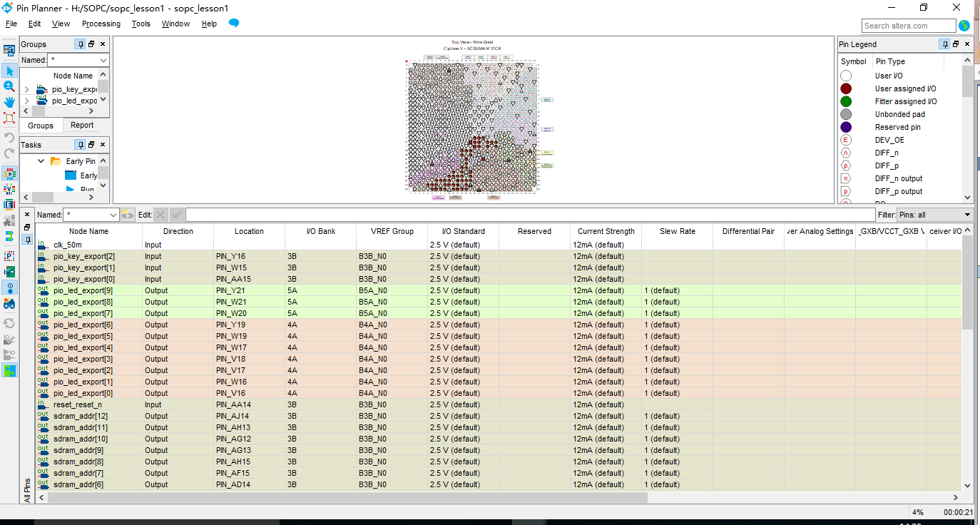
分配引脚:
到这里,整个板载部分逻辑设计及nios相关的设计就完成了,下面即是编写EDS文件然后进行仿真。
编写EDS工程:
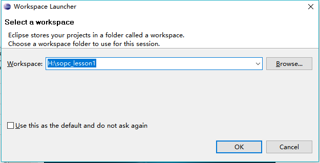
打开tool->NIOS II Software Build Tools for eclipse 并将workspace设定到自己本次工程的目录下
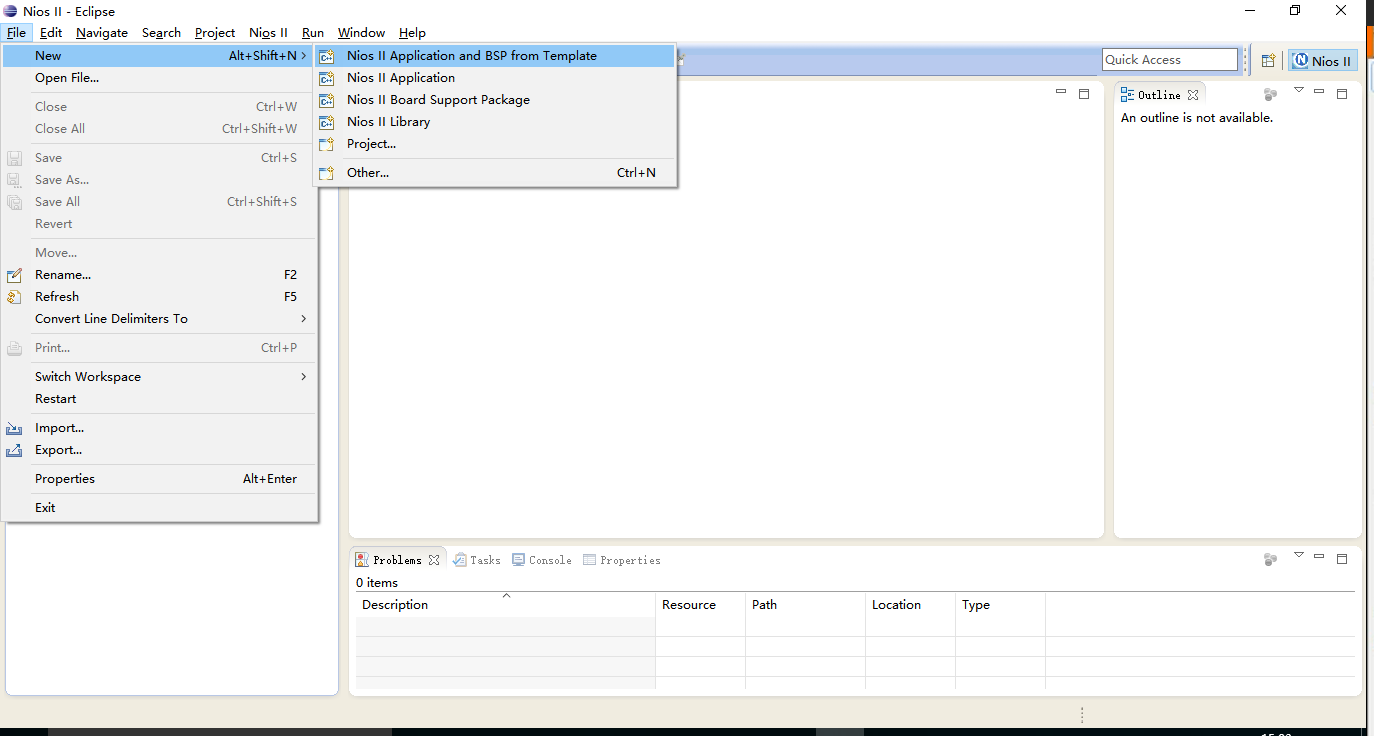
选则创建模板和bsp工程

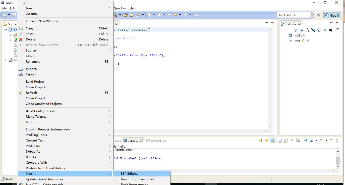
对nios_bsp进行设置
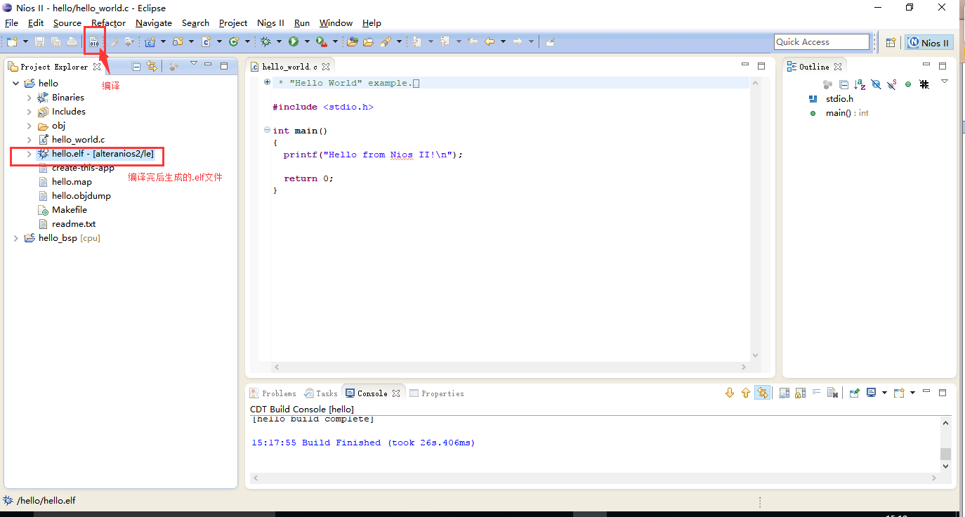
发现其已经默认设置好了uart_0为输出,默认即可,所以退出。
编译整个工程
烧写.sof文件

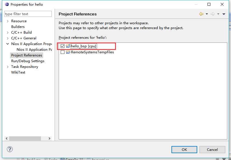
设置关连文件,将hello与bsp关联起来
烧写.elf文件
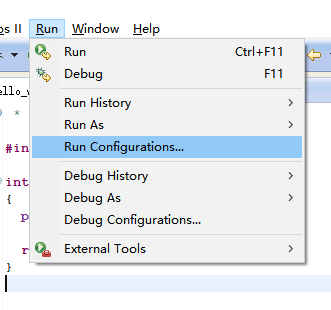
选择project
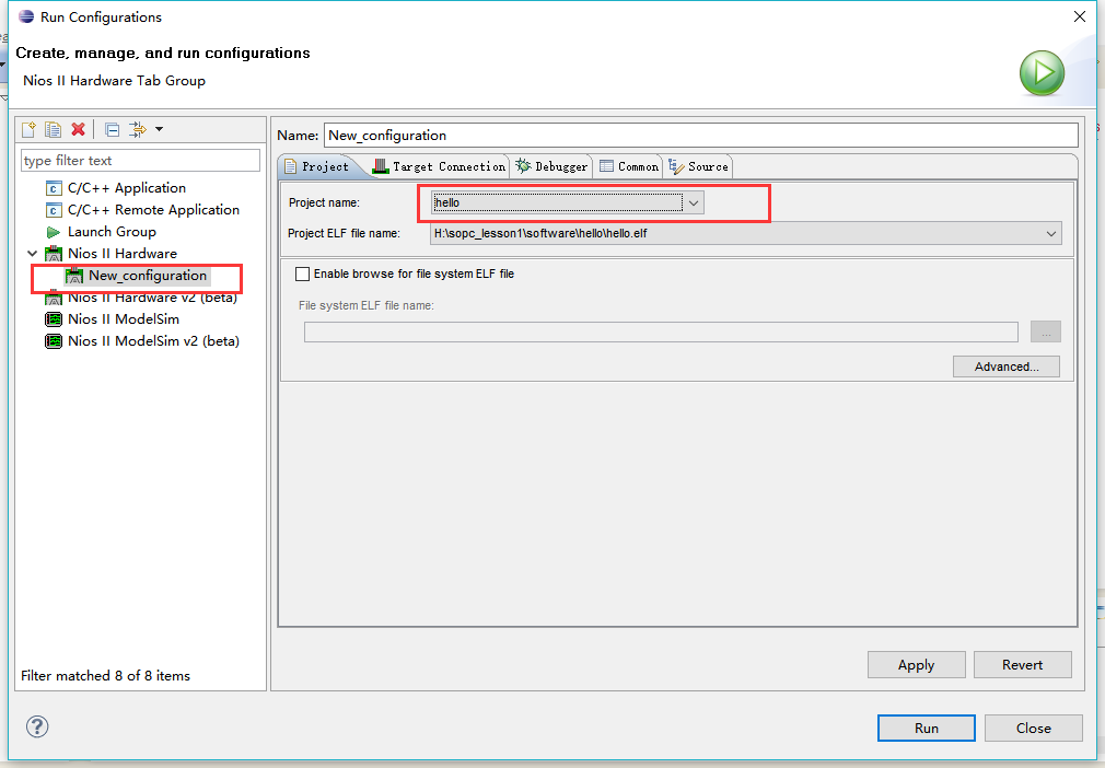
执行下面这步,点击运行
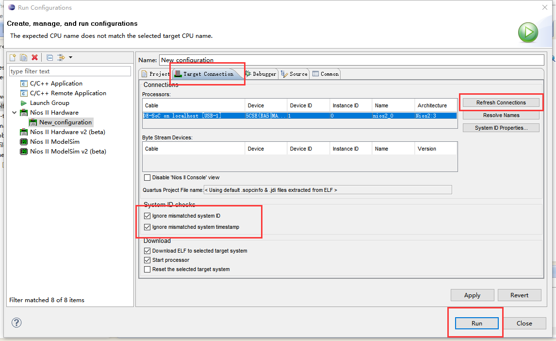
至此程序烧写完成。

实验现象:
将USB-TTL按照GND->GND
TXD->GPIOD0
TXD->GPIOD1
串口调试助手波特率设为9600
.sof文件烧写进开发板时,led灯全亮,按复位键串口调试没有数据接收,

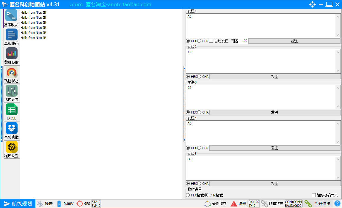
将.elf文件烧写到FPGA后,按下KEY0,串口调试助手接收到信息如图
最后对hello_world.c进行如下编程,完成对I/O和基本函数的调用
/*
 * "Hello World" example.
 *
 * This example prints 'Hello from Nios II' to the STDOUT stream. It runs on
 * the Nios II 'standard', 'full_featured', 'fast', and 'low_cost' example
 * designs. It runs with or without the MicroC/OS-II RTOS and requires a STDOUT
 * device in your system's hardware.
 * The memory footprint of this hosted application is ~69 kbytes by default
 * using the standard reference design.
 *
 * For a reduced footprint version of this template, and an explanation of how
 * to reduce the memory footprint for a given application, see the
 * "small_hello_world" template.
 *
 */

#include <stdio.h>
#include <system.h>//添加包含了系统宏定义的文件
#include <altera_avalon_pio_regs.h>//添加包含IO操作函数的.h文件
#include <unistd.h>//添加包含usleep的头文件进行精确延时

int main()
{
  printf("Hello from Nios II!
");
  while(1)
  {
  IOWR_ALTERA_AVALON_PIO_DATA(PIO_LED_BASE,0);//通过向PIO的基地址写数据,实现对GPIO的控制
  //delay(1000000);
  usleep(1000000);//us级延时
  IOWR_ALTERA_AVALON_PIO_DATA(PIO_LED_BASE,0x3ff);//通过向PIO的基地址写数据,实现对GPIO的控制
//  delay(1000000);
  usleep(1000000);//us级延时
  }
  return 0;
}
同样的方法再次烧写程序
实验现象:LED以2HZ的频率闪烁

